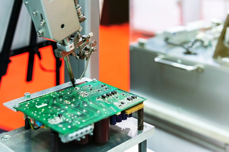
PCB Layout Checklist: Placement, Routing and Rule Checks
A PCB layout checklist is useful for the same reason it is useful in an aircraft cockpit: it protects against the failure mode of a competent person concentrating on one thing and forgetting another. Layout work invites exactly that failure, because the task is long, the tool is full of features, and the consequences of a missed item appear weeks later on a fabricated board. The list below is organised by the stage at which each check applies, so that it can be used as a working document rather than read once.
Placement Checks
Placement decides most of what follows, so it deserves the largest share of the review. Every component should be placed, and the placement boundary should be displayed on both the top and bottom layers so that overlap is visible as a design rule check rather than as a drawing error. Fiducials should be present, correctly sized and sufficient in number for the placement and paste printing machines. Heavy components belong near a board support point or a supported edge, where they will not bow the laminate. Components associated with an interface should sit near that interface, and a bus driver for a backplane should sit near the backplane connector, because the distance decides how much the stub costs in signal quality.
Mechanical details are just as important. Around a press-fit socket, no component on the component side should be taller than the socket within about five millimetres, and on the opposite side the area should be free of components and solder joints. Parts with metal cases need clearance from neighbouring components so that they cannot touch. Components that must be hand soldered should be limited in number, and tall axial parts are often better laid horizontally, with a retaining feature such as a fixed pad for a crystal. Where a heat sink is required, the clearance around it and the height of the parts beneath it both have to be confirmed. Devices that are part of the structure should be locked once placed so that they cannot be moved accidentally.

Functional Grouping and Signal Flow
Mixed-signal boards should have their digital and analog sections separated, and the signal flow within each section should be sensible rather than merely non-overlapping. A converter that spans the boundary should be placed so that its digital pins face the digital section and its analog pins face the analog section. Clocks and high-speed devices belong where their nets are short and their reference planes are continuous. Termination components have specific positions that follow from their function: a series resistor at the source belongs at the driver, a middle termination belongs at the midpoint, and an end termination belongs at the receiver. Where a signal must cross a plane split, the stitching component that connects the two reference planes should be close to the crossing. Protection devices should be arranged so that the circuit can be divided as intended, and a fuse on a board supply belongs near the connector with no component ahead of it.
Signal levels also constrain placement. A strong signal and a weak signal, defined as a difference of roughly 30 dB, should be laid out in separate areas rather than interleaved. The decoupling capacitor for each integrated circuit has to be placed as part of the placement review rather than left to the routing stage, because its position is what decides whether it works; the underlying mechanism is described in this article on placement order and pad positioning. Where a component exists specifically to influence electromagnetic behaviour, such as a reset circuit that must sit near its button, the placement requirement should be recorded with the component.
Thermal Checks
Thermally sensitive parts, including electrolytic capacitors and crystals, should be kept away from power devices and heat sinks, and the layout should follow the cooling path that the mechanical design provides. That means checking not only the placement of the hot parts but the direction of the airflow they sit in, because a component placed downstream of a heat source runs hotter than the same component placed upstream. Where the mechanical design defines an airflow channel, the layout should be reviewed against it rather than against the board alone.
Power Checks
Supply-related checks are quick and often decisive. The distance from a regulator or module to the devices it feeds should be short enough that the distribution network behaves as intended, and the decoupling around a regulator or a module supply should be placed according to the device requirements rather than by habit. The overall arrangement of the power section should keep the high-current loop small and the return path continuous, and the placement of the parts that carry the largest currents should reflect the current they carry rather than the convenience of the drawing.

Constraint and Rule Setup
Before the board is routed, the rules that will govern it should already exist. All simulation-derived constraints should be present in the constraint manager, and the physical and electrical rules should be defined, with particular attention to the power and ground nets, which are often treated as special cases. The spacing reserved for test vias and each test point must be adequate for the probe being used. The stackup should be checked against both the electrical requirement and the fabricator”s capability, and every differential pair that has an impedance requirement should have that impedance calculated and enforced by a rule rather than drawn by eye. A design rule check is only as good as the rules behind it.
Post-Routing Checks
Once the routing is complete, a second set of checks applies. Digital and analog routing should remain separated, and where the ground is split, a signal crossing between the two sections should use the bridge point rather than crossing anywhere convenient. Signals that must cross between split power areas should reference a continuous ground plane. Clock nets should run on inner layers wherever possible, and clocks, high-speed nets, reset lines and other radiating or sensitive nets should follow the 3W spacing rule, described in this article on the 3W rule for crosstalk. Low-level differential signals such as a low-voltage differential pair should be separated from single-ended logic by about ten times the trace height above the reference plane. Clock and high-speed traces should avoid regions dense with vias and should not be routed between the pins of a fine-pitch device.
Clock nets deserve their own final check: as few vias as possible, short overall length, a continuous reference plane preferably on a ground layer, a ground via within about 200 mil of any layer change that switches the ground reference, and a decoupling component within the same distance where the layer change moves to a different reference voltage. No stub should hang from a clock, reset, high-speed or Ethernet net, including test points added for convenience. Where the board is mixed-signal, the separation and return rules in this article on mixed-signal PCB design guidelines provide the reasoning behind these items.
FAQ
How long should a layout review take? The mechanical and functional checks take about an hour on a moderately complex board. The value comes from running the same list every time rather than from a long list run once.
Why does a decoupling capacitor need to be checked at placement rather than routing? Because its effect depends on the loop it forms with the supply and ground pins. A capacitor that is placed correctly cannot be ruined by routing, while one placed badly cannot be rescued.
What is the most commonly missed item? Items with no electrical symptom, such as probe access, socket clearance and the position of a heat sink relative to the parts beneath it.