PCB Layout and Routing: A Practical Order of Operations
A board that is easy to route is usually a board that was planned before it was routed. The order of operations matters more than any individual rule: floor plan first, then connectors, then the parts that join functions, then the zoning rules that keep noisy circuits away from sensitive ones. Engineers who skip the first step spend the time later, in rework, in extra layers, and in boards that work on the bench but fail in the field.
Start from a modular floor plan
The first principle of layout is easy to state and hard to follow: the division into modules should be obvious. Anyone with basic circuit knowledge should be able to look at the board and say which area performs which function. A clear floor plan is also what makes review possible, because a reviewer can check one block at a time instead of holding the whole board in mind.
The practical sequence starts from the schematic. Generate the initial board file, complete a rough pre-layout to establish the relative area each function needs, and pass those areas to the mechanical designer. The mechanical constraints that come back, together with the overall product architecture, then define the board outline, the mounting openings, and the keep-out zones that routing must respect.
Only after those boundaries exist does placement begin. The boundary drawing is not a formality: it is what turns an open-ended placement problem into a bounded one, and it is the reason a floor plan can be reviewed at all.

A floor plan that cannot be explained in one sentence per block is usually a floor plan that will be re-done.
Place the controller and the interfaces
The main controller normally sits near the centre of the board. From there, the distance to every peripheral block is roughly equal, which keeps the longest trace on the board as short as it can be. Interface circuits are then placed against their connectors, so that a network port, a USB connector, or a video connector sits immediately behind its own magnetics, protection, and filtering.
Almost every interface needs electrostatic discharge protection and filtering, and the order is not negotiable: protection first, then filtering. A filter placed ahead of a protection device is exposed to the full transient, and a protection device placed after a filter has to survive a waveform the filter has already degraded. Getting this order right at placement time costs nothing; getting it wrong costs a board revision.
Then place the power architecture
The main supply conversion stage belongs at the power entry point, where the input connector feeds the board. A 5 V input, for example, is converted close to where it enters, which keeps the high-current input loop short. Secondary regulators that generate local rails, such as a 2.5 V rail used by one module, can be placed near the loads they serve, even when they draw from the same supply network.
Placement of the supply also sets the reference for the return current. A converter that is far from its load pushes a high-current loop across the board, and that loop is an antenna. Shortening it is one of the few layout decisions that improves efficiency, noise, and electromagnetic performance at the same time.
Zone by function and by speed
Inside the planned areas, zoning rules do the real work. High-speed circuits are separated from low-speed circuits, analog from digital, and sources of interference from sensitive receivers. Internal circuits that never reach a connector follow the same logic, which is why the division is usually described in three pairs: speed, signal type, and noise character.
Individual modules are then laid out along the path the current takes in the schematic. Input filter, conversion stage, load, and return each occupy a region along that path, so the physical arrangement mirrors the electrical one. When the physical order matches the current flow, the routing between stages becomes short and the return path stays under the trace that created it.
Route for validity, not only connectivity
The basic requirement of routing is that every net is connected, and that part is easy. The harder requirement is that each connection is valid, and validity means something different for each signal type. In a digital circuit it means enough noise margin for the receiver to recognise the level; in an analog circuit it means as close to zero loss as the design allows.
Both goals are reached the same way, by controlling the impedance and the return path. A digital trace that is routed over a split plane has a return path that detours, which raises the loop inductance and eats the margin. An analog trace that shares its return path with a switching supply picks up the switching waveform directly.
Assign layers before drawing traces
Layer assignment is a planning step, not a routing step. The usable signal layers should be ranked before work begins: a best layer that sits directly against a complete ground plane, then the second-best layers beneath it. Critical nets belong on the best layer, including the full memory bus of a high-speed interface, differential pairs, and analog signals.
Everything else can share the remaining layers. Slower interfaces and general purpose I/O belong on ordinary layers, and a critical region should carry only the signals that belong to it, so a memory bus area holds the memory bus and nothing else. The stackup itself is worth planning early; the trade-offs between layer counts and reference plane quality are covered in layer stackup from one to eight layers.
Impedance, reflection, and crosstalk
High-speed routing has to answer three questions at once: reflection, crosstalk, and electromagnetic compatibility. Impedance matching is the tool for reflection, and the targets are set by the interface: a single-ended line is commonly controlled at 50 ohm and a differential pair at 100 ohm, with the final numbers taken from the actual design. The principle behind the number is that impedance should be equal along the line and continuous through every transition.
Crosstalk is controlled primarily by spacing and by the reference plane. The 3W and 2W spacing rules and grouped ground treatment cover most cases, and the same geometry that controls crosstalk also limits the loop area that radiates. Our guide to the 3W rule works through the spacing arithmetic.
Keep the power loop thick and short
Power circuits are designed for current capacity first. The entire supply loop, from source through the load and back, should be as wide and as short as the layout allows, because a narrow long loop adds resistance, inductance, and heat at the same time. From an electromagnetic standpoint the loop is an antenna, so reducing its enclosed area reduces both emission and susceptibility.
Copper area is not the only variable. The number of vias, the width of the necks between planes, and the length of the path that runs parallel to a return path all affect the loop. Trace width for a given current is a calculation rather than a guess, and the method is set out in trace width and current calculation.
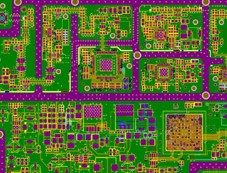
Return paths should be planned at the same time as the traces they belong to, because a return path that is discovered after routing is a return path that cannot be fixed.
Plan the ground system
Ground is the reference plane, and if the grounding is wrong nothing above it is stable. The first split is between chassis ground, which the product metalwork connects to, and system ground, which is the reference for the circuits. The usual arrangement keeps them separate and joins them at defined points, through a ferrite bead or a high-voltage capacitor, instead of tying them together everywhere.
System ground is then divided functionally into digital, analog, and power sections. Whether that division should also be physical is a long-running argument, and the answer depends on the layout. If the placement is good, with the digital area carrying only digital signals, the analog area only analog signals, the supply area only supply signals, and a complete ground layer underneath, the ground can be split safely. Each return current flows down to the plane beneath it and back to its source by the shortest route.
When placement is not that clean and signals cross between regions, a single tie point is usually better. A 0 ohm resistor at the densest crossing point, where the circulating area is smallest, is the common choice. A ferrite bead is often avoided in that position because it filters at high frequency and shifts the reference. Decisions of this kind on the supply side are covered in power plane splitting rules.
Applying the sequence on a real project
The order described here is not a workflow document; it is the sequence that keeps rework off the schedule. PCB layout and routing decisions made in the wrong order cost the most, because a floor plan that changes after routing invalidates the routing, while a trace that changes after placement costs only the trace. Component placement therefore deserves the time it takes, and the zoning rules that follow it should be treated as constraints rather than as suggestions.
FAQ
Which comes first, placement or stackup? They inform each other, but placement sets the constraint. Decide the regions and the critical interfaces first, then choose the stackup that gives those interfaces a continuous reference plane.
How many layers do I need? Enough that every critical net has a complete plane beneath it. Once the interfaces and the pin density fix the layer count, layer assignment becomes a matter of ranking rather than of adding copper.
Can routing fix a bad floor plan? Rarely. Routing can improve a good plan and cannot rescue a poor one. If two noisy blocks share an area, the fix is to move one of them.