What Drives PCB Manufacturing Cost: Layers, Vias and Materials
Layout effort goes into placement and routing, and the cost that the layout creates is usually noticed later, when the quotation arrives. Most of that cost is decided by a small number of choices, and almost all of them can be made deliberately rather than by default. Knowing which ones carry a surcharge is what turns PCB manufacturing cost into something the designer controls.
Layer Count
The number of layers is the largest single factor. Routing becomes easier with every layer added, because more routing channels are available and the power distribution can be moved to dedicated planes, and the price rises roughly in proportion to the count. A design that grows from four layers to eight can end up close to twice the price for the same outline.
The way to control it is to add layers only where they buy something specific: a reference plane under a controlled impedance layer, a power plane for a supply that cannot be distributed on the surface, or routing density that cannot be achieved otherwise. Two extra layers for convenience are a permanent cost on every board built.
Vias
The second factor is the drill programme. A via size of 0.25 mm diameter or larger is within the standard capability of most shops. Below that, the drill bits wear faster, the plating is harder to control and the registration tolerance tightens, so a surcharge is applied. Where the package pitch or the routing density does not force a smaller via, keeping the via at or above that size is a straightforward saving.
A via that is placed inside a pad, the so-called via in pad, is a separate case. It has to be filled and plated over to give a flat surface for the paste deposit, which adds a process step and a yield risk. It is sometimes unavoidable, for example under a fine pitch package where there is no room to escape to a via beside the pad, but it should never be used because it is convenient.
Back drilling is used to remove the unused stub of a via in thick backplanes and on boards with very high speed signals. The stub that remains after conventional drilling behaves as a resonant line and limits the bandwidth of the through connection, and removing it restores the performance. The process adds roughly ten to twenty percent to the board price, which is easy to justify on a high-speed backplane and hard to justify anywhere else.
Trace Geometry
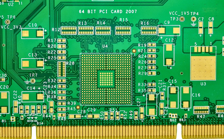
Line width and spacing follow the same logic as via size. Above the standard minimum, the process is comfortable; below it, the imaging, the etching and the copper thickness control all become more critical. The usual threshold where a surcharge begins is in the region of 3.5 mil for both width and spacing, so a design that can be routed at a slightly wider geometry avoids the premium. Where the impedance target demands a narrow trace, the target is what it is, but the surrounding traces can often be widened.
Copper thickness belongs here as well. Heavier copper carries more current and spreads heat, and it also makes fine geometry harder to etch, so a board with heavy copper usually comes with a relaxed minimum width.
Base Material
The laminate is the third cost driver. Standard FR-4 is the default, and anything that deviates from it raises the price: a high glass transition temperature for a board that will see high soldering temperatures or a harsh environment, a halogen-free material for a product with that requirement, or a high-frequency laminate with a low loss tangent for RF and microwave work.
The increase comes partly from the material price and partly from the purchasing cycle, because an unusual laminate may not be stocked and has to be ordered in a minimum quantity. One useful technique is to use the special material only where it is needed. A radio section can be built on a high-frequency laminate while the digital section uses FR-4, and the two can be pressed into one board as a hybrid stack, which reduces the amount of expensive material to the area that benefits from it.
HDI and Blind or Buried Vias
The largest single increase in price comes from HDI construction. Laser drilled microvias, stacked or staggered vias, and any structure that requires the board to be built and laminated in more than one press cycle, all raise the cost substantially.
It is worth checking whether the construction is actually required before accepting it. A BGA with a pitch of 0.65 mm or larger can normally be fanned out with through vias, because the diagonal space between four balls is enough for a single via and a short escape trace. Some 0.5 mm pitch packages can also be fanned out with through vias, depending on the pad size and on which pins carry signals. The decision depends on the pad geometry and the pin distribution rather than on the pitch alone, and it is worth calculating rather than assuming.
Where HDI is required, it is usually required for a specific device rather than for the whole board. Keeping the microvia region local to the fine pitch device, and using conventional construction elsewhere, is a cheaper arrangement than making the whole board HDI.
Surface Finish
The finish protects the copper before soldering and determines how well the assembly process can wet it.
Hot air solder levelling is the cheapest and is adequate for through-hole and coarse surface mount work. Electroless nickel immersion gold gives a flat surface that suits fine pitch assembly, wire bonding and long storage, and it costs more. Immersion tin and immersion silver are flat finishes that sit between the two in price and are used for fine pitch assembly without the bonding requirement. Hard gold on the edge connector, or gold fingers, is a separate selective finish that is plated only where the connector contacts need to survive repeated insertion.
The choice should follow the product. Paying for gold on a board that will be soldered once and mounted inside an enclosure is paying for storage life and flatness that the product may not need, and using hot air levelling on a board with 0.4 mm pitch parts is a false economy.
What Else Moves the Price
Several factors are not design choices in the layout but still belong in the calculation.
Panel utilisation matters as much as board area, because the shop pays for the panel rather than for the board. An outline that tiles badly wastes material on every order. The quantity in each order, the lead time, the acceptance of a standard panel size and the willingness to combine orders across a build all change the unit price, and our PCB manufacturing team works through those trade-offs with the customer before quoting.
Impedance control is a design requirement that becomes a fabrication requirement: the shop has to test coupons and control the dielectric thickness, which adds cost. Where an impedance target is genuinely needed it is worth the money, and where it was copied from an earlier design it is worth checking before paying for it. The constructions we build and the tolerances we hold are listed on our PCB capabilities page.
The last consideration is how the cost is spent. Saving a few percent on the board and losing a build to a design that does not assemble is not a saving, which is why the review that reduces cost is the same review that improves yield. Where a design is costed for volume, the same review runs across the whole product rather than the bare board, and the assembly decisions are made with the board decisions in our high volume PCB assembly programmes.
FAQ
What single change reduces the price most? Reducing the layer count, if the electrical requirement allows it. It is the largest proportional cost in the board.
Is a small via always more expensive? Below the standard minimum, yes. A via of 0.25 mm or larger is normally within the standard process and carries no premium.
Does HDI always cost more? Yes, and by a large margin, because it requires additional lamination cycles and laser drilling. Check whether a through via fanout is possible before committing to it.