PCB Manufacturing: How to Choose the Right PCB Manufacturer
What Is a PCB Manufacturer?
A PCB manufacturer converts an electronic design into a physical printed circuit board that can be assembled with electronic components. From smartphones and computers to industrial controllers, medical equipment, automotive electronics, communication systems, and AI hardware, PCBs provide the electrical and mechanical foundation for modern electronic products.
As electronic systems become smaller, faster, and more complex, PCB manufacturing requires much more than simply etching copper onto a laminate. A capable manufacturer must coordinate material selection, circuit imaging, drilling, copper plating, lamination, solder mask, surface finishing, electrical testing, inspection, and final quality control.
The right manufacturing partner should also understand how PCB fabrication affects downstream assembly and product reliability.
For engineers and purchasing teams, selecting the right supplier is therefore an important part of product development and supply-chain management.
Why Does the PCB Manufacturer Matter?
PCB quality directly affects electrical performance, assembly yield, product reliability, and production cost.
A board may meet its basic dimensional requirements but still create problems if the manufacturer cannot consistently control:
- Trace width and spacing
- Copper thickness
- Via dimensions
- Layer registration
- Dielectric thickness
- Impedance
- Surface finish
- Solder mask registration
- Warpage
- Hole quality
- Electrical continuity
These variables become increasingly important as PCB designs move toward higher layer counts, finer geometries, smaller vias, higher frequencies, and more demanding thermal environments.
A reliable manufacturer should therefore provide both process capability and engineering support, rather than simply offering a low fabrication price.
Key Capabilities of a Professional PCB Manufacturer
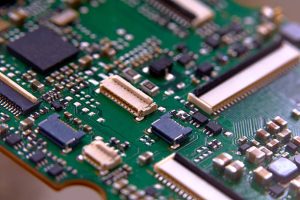
When evaluating a PCB manufacturing company, it is useful to examine its capabilities across several areas.
1. Multilayer PCB Manufacturing
Multilayer PCBs allow designers to integrate more circuits into a smaller area by using multiple conductive layers separated by dielectric materials.
A professional manufacturer should have experience with:
- 4-layer and 6-layer PCBs
- High-layer-count boards
- Controlled-impedance designs
- Blind and buried vias
- Sequential lamination
- Fine-line circuitry
- Complex stackups
- High-density interconnect structures
For demanding products, the manufacturer should be able to review the stackup before production and identify potential manufacturing or signal-integrity problems.
GOPCBA provides a broad range of PCB Manufacturing services covering prototype and production requirements.
PCB Materials and Application-Specific Selection
Material selection is one of the most important decisions in PCB manufacturing.
Standard FR-4 is suitable for a wide range of electronic applications, but it is not the ideal solution for every design.
Depending on application requirements, engineers may consider:
- Standard FR-4
- High-Tg FR-4
- High-speed laminates
- High-frequency materials
- Flexible materials
- Rigid-flex materials
- Aluminum or other metal-core constructions
- Specialized low-loss dielectric materials
High-Frequency and High-Speed Applications
High-speed digital and RF designs require careful consideration of dielectric constant, dissipation factor, copper roughness, dielectric thickness, trace geometry, and impedance.
Using a suitable low-loss material can help control insertion loss and signal distortion, but material selection should always be evaluated together with the complete stackup and routing structure.
Thermal Applications
When heat dissipation is a major design requirement, metal-core PCB constructions or other thermal-management solutions may be appropriate.
The correct material depends on the thermal load, electrical isolation requirements, operating temperature, mechanical structure, and overall system design.
Advanced PCB Manufacturing Processes
Technology capability is another important factor when selecting a PCB supplier.
Laser Direct Imaging
Laser direct imaging can support fine-line circuit fabrication by directly imaging the circuit pattern onto the photoresist.
It is particularly useful for designs requiring tighter geometries and improved registration control.
Precision Drilling
Mechanical drilling and laser drilling are both important PCB manufacturing technologies.
Mechanical drilling is widely used for conventional through-holes, while laser drilling can be used for smaller microvias and certain HDI structures.
The correct drilling technology depends on:
- Hole diameter
- Board thickness
- Aspect ratio
- Layer structure
- Via type
- Material system
Copper Plating
Copper plating establishes the conductive structure required for interlayer connections and plated through-holes.
Process control is essential because inconsistent copper deposition can affect electrical performance and reliability.
Important parameters include:
- Plating thickness
- Hole-wall coverage
- Current distribution
- Chemical bath condition
- Surface preparation
- Panel uniformity
PCB Surface Finishes
The surface finish protects exposed copper and provides a suitable surface for component assembly.
Common PCB surface finishes include:
ENIG
Electroless Nickel Immersion Gold provides a relatively flat surface and good oxidation resistance. It is frequently selected for fine-pitch components and applications where surface flatness and storage stability are important.
HASL
Hot Air Solder Leveling is a widely used and economical surface finish. Lead-free HASL is commonly selected for RoHS-compliant applications.
OSP
Organic Solderability Preservative provides a thin protective layer over copper and can be a cost-effective option for many soldering applications.
ENEPIG
Electroless Nickel Electroless Palladium Immersion Gold can be considered for demanding applications requiring enhanced surface performance and compatibility with advanced assembly technologies.
The best surface finish depends on the assembly process, component pitch, storage conditions, reliability requirements, and cost target.
Quality Control in PCB Manufacturing
Quality control should cover the complete production process, from incoming materials to final inspection.
A professional PCB manufacturer should establish inspection checkpoints throughout production.
Automated Optical Inspection
AOI systems can inspect PCB patterns for defects such as:
- Open circuits
- Short circuits
- Missing copper
- Excess copper
- Pattern abnormalities
- Solder mask-related defects
X-Ray Inspection
X-ray inspection can be useful for examining internal structures that cannot be evaluated through conventional visual inspection.
It is particularly valuable for complex multilayer structures and certain advanced PCB constructions.
Electrical Testing
Electrical testing verifies circuit continuity and isolation according to the manufacturing requirements.
Depending on the design and production volume, manufacturers may use flying-probe testing, fixture-based testing, or other electrical test methods.
Cross-Section Analysis
Cross-sectional inspection can help evaluate internal PCB construction, including:
- Copper plating
- Dielectric thickness
- Hole-wall structure
- Layer registration
- Lamination quality
- Via structure
For demanding applications, this provides valuable process-validation information.
Why DFM Matters Before PCB Production
One of the most effective ways to reduce PCB manufacturing problems is to identify them before fabrication begins.
Design for Manufacturability (DFM) reviews the PCB design against the actual manufacturing process.
Typical DFM checks include:
- Minimum trace width
- Minimum spacing
- Hole diameter
- Hole-to-copper clearance
- Annular ring
- Solder mask clearance
- Silkscreen positioning
- Copper distribution
- Stackup feasibility
- Impedance requirements
- Panelization
- Manufacturing tolerances
An experienced manufacturer should communicate potential problems before production rather than discovering them after boards have already entered fabrication.
GOPCBA’s PCB Design and Layout Engineering services can support design review, layout optimization, DFM considerations, and production-file preparation.
PCB Prototyping Before Mass Production
PCB prototyping is an important stage in product development.
A prototype allows engineers to verify:
- Electrical functionality
- Mechanical dimensions
- Component placement
- Signal integrity
- Thermal behavior
- Assembly compatibility
- Connector alignment
- Manufacturing feasibility
Prototype production can also reveal design problems that may not be obvious in CAD software.
For example, a designer may discover that a particular via arrangement is difficult to manufacture, that a component pad geometry creates soldering problems, or that a stackup requires adjustment to achieve the intended impedance.
For these reasons, prototype fabrication and assembly should ideally be evaluated as one development cycle.
A dedicated Prototype PCB Assembly workflow can help engineers validate both the bare PCB and assembled board before committing to larger production quantities.
PCB Manufacturing for High-Frequency and High-Speed Electronics
Modern communication, computing, networking, radar, and RF products place demanding requirements on PCB manufacturing.
For high-frequency applications, designers need to consider more than just trace dimensions.
Important factors include:
Dielectric Properties
The dielectric constant and dissipation factor influence signal propagation and loss.
Copper Surface Roughness
At higher frequencies, conductor surface characteristics can contribute to additional transmission loss.
Controlled Impedance
Transmission-line geometry must be controlled according to the target impedance.
Layer Registration
Small registration errors can affect controlled-impedance structures and high-density interconnections.
Material Consistency
Variations in dielectric thickness and material properties can influence electrical performance from one production batch to another.
A PCB manufacturer with experience in high-speed and high-frequency fabrication should therefore participate in the engineering review instead of treating the design as a standard board.
PCB Manufacturing for Automotive, Industrial, Medical, and Communication Applications
Different industries impose different PCB requirements.
Automotive Electronics
Automotive PCBs may need to withstand thermal cycling, vibration, humidity, and long operating lifetimes. Manufacturing consistency and traceability are especially important.
Industrial Control
Industrial control boards often operate continuously and may be exposed to electrical noise, temperature changes, and demanding environmental conditions.
Medical Electronics
Medical PCB applications can require strict quality management, traceability, reliability, and manufacturing consistency depending on the product.
Communication Equipment
Communication hardware frequently requires controlled impedance, low-loss materials, high layer counts, and precise signal-integrity control.
This is why choosing a PCB supplier based solely on price can be risky. The supplier’s experience with the target application is equally important.
From PCB Fabrication to PCB Assembly
PCB fabrication is only one stage of electronics manufacturing.
After the bare board is produced, components must be sourced and assembled. Managing fabrication and assembly through separate suppliers can increase communication requirements and make responsibility for quality less clear.
An integrated manufacturing partner can support:
- PCB fabrication
- Component sourcing
- SMT assembly
- Through-hole assembly
- Reflow soldering
- Inspection
- Electrical testing
- Final assembly
For customers looking for a single manufacturing workflow, Turnkey PCB Assembly can combine PCB fabrication with component procurement and assembly services.
How to Evaluate a PCB Manufacturer
Before selecting a supplier, purchasing and engineering teams should evaluate several factors.
Manufacturing Capability
Confirm that the manufacturer can produce the required:
- Layer count
- Board thickness
- Trace/space
- Hole sizes
- Via structures
- Copper weights
- Materials
- Surface finishes
Quality Management
Ask about quality certifications, inspection systems, electrical testing, traceability, and corrective-action procedures.
Engineering Support
A strong supplier should be able to review Gerber files, drawings, stackups, and manufacturing requirements.
Prototype Capability
Prototype support is important for new product development and design validation.
Production Scalability
The supplier should be able to transition from prototype quantities to repeat production without significant changes in process control or quality standards.
Communication
Clear communication is essential when specifications, engineering changes, delivery schedules, or quality issues need to be resolved quickly.
Common Mistakes When Choosing a PCB Manufacturer
Choosing Only by Price
The lowest quotation does not necessarily represent the lowest total cost.
Poor quality can result in scrap, assembly defects, delays, redesigns, and field failures.
Ignoring Engineering Capability
A manufacturer without sufficient engineering support may simply build the supplied files without identifying manufacturability risks.
Failing to Verify Materials
Equivalent-looking materials may have significantly different electrical, thermal, or mechanical characteristics.
Material specifications should be clearly documented.
Skipping Prototype Validation
Moving directly from design to mass production can increase the risk of expensive production changes.
Not Considering Assembly
The bare PCB should be designed and manufactured with the final assembly process in mind.
PCB Manufacturing Cost Factors
PCB price is influenced by many variables, including:
- Board dimensions
- Layer count
- Material type
- Copper thickness
- Board thickness
- Trace and spacing requirements
- Hole size
- Via technology
- Surface finish
- Quantity
- Testing requirements
- Panel utilization
- Production lead time
A high-layer-count PCB with fine-line circuitry and advanced materials will naturally have different manufacturing economics from a standard two-layer FR-4 board.
The best purchasing decision is therefore based on total value rather than unit price alone.
What Information Should You Send to a PCB Manufacturer?
To receive an accurate quotation and engineering review, customers should normally provide complete manufacturing information.
Typical files include:
- Gerber files
- Drill files
- PCB fabrication drawing
- Stackup information
- Material requirements
- Copper thickness
- Surface finish
- Solder mask requirements
- Electrical testing requirements
- Special manufacturing instructions
- Quantity requirements
For complex projects, a detailed fabrication drawing and stackup can significantly reduce ambiguity during quotation and production.
Why Choose GOPCBA for PCB Manufacturing?
A capable PCB manufacturing partner should support the complete product-development cycle, from engineering review and prototype fabrication to production and assembly.
GOPCBA provides PCB manufacturing and electronics manufacturing services designed for customers requiring reliable fabrication, engineering support, and scalable production.
The manufacturing workflow can support different PCB technologies, materials, layer structures, surface finishes, and assembly requirements according to project specifications.
For companies developing new electronic products, the combination of PCB fabrication, prototype assembly, component sourcing, and production support can simplify supplier management and shorten the path from design to finished electronics.
Conclusion
Choosing the right PCB manufacturer is an engineering and supply-chain decision, not simply a purchasing decision.
A reliable supplier should combine manufacturing capability, material expertise, process control, inspection systems, engineering support, prototype services, and production scalability.
For standard boards, basic manufacturing capability may be sufficient. However, advanced products involving high-speed signals, high-frequency circuits, HDI structures, high layer counts, thermal management, or demanding reliability requirements require a much more capable manufacturing partner.
The most effective approach is to evaluate the supplier against the complete product lifecycle:
Design → DFM Review → PCB Prototyping → Fabrication → Inspection → Assembly → Testing → Production
By selecting a PCB manufacturer capable of supporting this complete workflow, electronics companies can reduce manufacturing risks, improve product consistency, and build a more reliable path from prototype to volume production.