PCB Manufacturing Parameters: Process Capabilities and Tolerances
Why PCB Manufacturing Parameters Decide Quality
A PCB’s quality does not depend only on the schematic and layout. During production the manufacturer must control many PCB manufacturing parameters, including board thickness, copper weight, line width and spacing, hole size, annular ring, impedance, surface finish, solder mask, plating thickness and dimensional tolerances. Engineers who understand these PCB process parameters are far more likely to design a board that is manufacturable, reliable and cost effective.
A design that looks perfect in CAD can still fail in the factory if key dimensions exceed the manufacturer’s real capability. Etching defects, insufficient hole copper, layer misregistration, impedance deviation and assembly problems all start with specifications that were never matched to process reality. Industry standards such as the IPC family provide the common framework for design, manufacturing, inspection and acceptance, and combining PCB manufacturing parameters, tolerances and standards early reduces production risk and improves batch consistency.
gopcb applies these parameters through its PCB manufacturing service with full DFM review before tooling.
What Are PCB Manufacturing Parameters?
PCB manufacturing parameters are the dimensional, material, electrical, mechanical and process requirements that production must follow. They define the structure, performance and difficulty of the finished board. The most commonly controlled items are layer count, board thickness, copper weight and foil weight, minimum line width and spacing, minimum and plated hole sizes, blind and buried via dimensions, via in pad structures, annular ring, trace tolerances, board outline tolerances, layer to layer registration, impedance, dielectric thickness, surface finish, solder mask thickness and web, plated copper thickness, nickel and gold thickness, warp and twist, and electrical test requirements.
None of these parameters are independent. Adding copper weight changes etching behavior. Reducing line width and spacing increases the difficulty of pattern transfer and etching control. Adding layers raises the complexity of lamination, registration and impedance control. PCB manufacturing parameters therefore have to be reviewed across the whole process rather than one by one.
Why These Parameters Matter
Reasonable parameters affect three outcomes: manufacturability, reliability and cost.
Manufacturability. The design must match the factory’s process capability. Very small line width and spacing, ultra small mechanical holes, high aspect ratio vias, extreme registration accuracy and microvia structures all demand advanced equipment, and ordinary processes cannot hold them consistently. Understanding parameters before release prevents designs that can never be produced reliably.
Reliability. Parameters directly affect long term behavior. Insufficient copper increases trace resistance and temperature rise. Thin hole copper weakens mechanical and thermal reliability of the via. Incorrect dielectric thickness causes impedance deviation on high speed nets. Solder mask misregistration increases solder bridging risk. Every parameter is therefore a reliability input, not just production data.
Cost. The more demanding the parameters, the more complex the process. Ultra fine lines, microvias, blind and buried vias, high layer counts, thick copper, high frequency material, tight impedance, special finishes and strict tolerances all add cost. The best PCB manufacturing parameters satisfy the product requirement while keeping yield high and price reasonable, not the highest specification a supplier can quote.
Key PCB Manufacturing Parameters
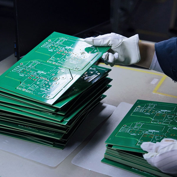
Layer count ranges from single and double sided to multilayer and high layer count stacks, and it controls routing space, impedance control and cost. Board thickness commonly spans 0.4 mm to 3.2 mm and above, balancing mechanical strength and assembly. Copper weight of 0.5 to 6 oz or higher sets current capacity and heat spreading. Minimum line width and spacing define the achievable routing density and yield, and hole size covers mechanical and laser drilled vias that determine connection reliability.
Annular ring ties hole and pad dimensions to via reliability, impedance values such as 50, 90 and 100 ohm control high speed signal integrity, and surface finish choices from HASL, ENIG and OSP to immersion silver affect solderability and shelf life. Solder mask thickness, openings and registration protect the surface, while dimensional tolerances decide how the board fits its mechanical assembly. There is no single standard value for every design, so the specific capabilities of the chosen factory and material system must be confirmed before production.
What Are PCB Manufacturing Tolerances?
PCB manufacturing tolerance is the allowed deviation between the actual produced dimension and the design nominal value. A board specified at 1.60 mm nominal thickness, for example, will not come out at exactly 1.60 mm but within the board thickness tolerance band.
Common tolerances cover board thickness, hole size and position, line width, outline dimensions, layer to layer registration, solder mask registration and impedance. Tight tolerances matter most for HDI, high speed, high density and precision assembly boards, where small deviations affect interlayer connection, impedance, mechanical fit and long term reliability. A design that only specifies nominal values without tolerances forces the factory to guess, and guessing always ends in disagreement.
Industry Standards for PCB Manufacturing
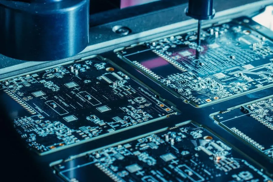
The IPC standards give a shared language between design and production. IPC-2221 covers generic PCB design, IPC-2222 applies to rigid boards, IPC-6011 defines performance categories, IPC-6012 specifies qualification and performance for rigid boards and IPC-A-600 sets acceptability criteria for the finished board. For assembly, IPC-A-610 is the common reference. Medical, automotive and aerospace programs add their own reliability requirements, and the applicable class, such as Class 2 or Class 3, must be agreed before quoting.
Standards are a baseline rather than a substitute for project specific decisions. Product class, customer specification, application environment, reliability goals and industry regulations should all be combined with the IPC references to define the real manufacturing requirements.
Parameters by Board Technology
Different technologies emphasize different parameters. Automotive PCBs focus on long term reliability, thermal cycling, vibration, material consistency, plating quality and process stability. RF and microwave boards care about dielectric constant, dissipation factor, copper foil roughness, impedance control and dielectric thickness consistency. HDI boards depend on microvia size, laser drilling, via in pad, fine lines, sequential lamination and layer registration. High current boards need copper weight, line width, thermal design and via current capacity, and high speed boards are defined by loss, impedance and stack-up control.
Because each technology has its own critical list, the DFM conversation should start from the application. gopcb supports multilayer, high speed, HDI, thick copper, high frequency, metal core, ceramic and industrial boards with engineering assistance on materials, stack-up, copper weight, line width, holes, impedance, finish and tolerances. A complete PCB design and layout package makes that review faster and more accurate.
Common Specification Mistakes
Specifying only the board thickness is the most common error. A 1.6 mm PCB is not fully defined until copper weight, material, dielectric structure, thickness tolerance and stack-up are included. The second mistake is unnecessary fine line work: if 5/5 mil satisfies the design, forcing 3/3 mil adds cost and yield risk for no benefit. Ignoring factory capability is next, so minimum line width, minimum hole, solder mask web, maximum copper and registration ability should be confirmed before design freeze. Overlooking tolerances on precision boards and treating IPC as the final answer instead of a reference are the last two common traps.
Complete manufacturing notes, a real DFM review and agreed tolerance callouts prevent rework and schedule delays. gopcb reviews every file through its PCBA testing and process qualification flow so the transition from prototype to volume stays predictable.
FAQ
Which PCB manufacturing parameters are most important? Board thickness, copper weight, layer count, line width and spacing, hole size, annular ring, impedance, surface finish, solder mask, plating thickness and dimensional tolerance.
What is the common PCB board thickness? 1.6 mm is a common nominal value, but 0.4, 0.8, 1.0, 1.2, 2.0 and 3.2 mm are also widely produced.
What is the standard PCB copper weight? 1 oz foil with about 35 micrometers nominal thickness is very common, and 2, 3, 4 oz or heavier copper is used for high current and power designs.
Which IPC standards apply to PCB manufacturing? IPC-2221, IPC-2222, IPC-6011, IPC-6012 and IPC-A-600 for boards, with IPC-A-610 for assembly.
How do parameters affect PCB price? Layers, copper, line width, holes, HDI structures, special materials, impedance, finishes and tolerances all raise process complexity and therefore cost.
Why are manufacturing tolerances important? They define the allowed deviation on the finished part, and on HDI, high speed and precision boards they directly affect connection, impedance, fit and reliability.
Get a DFM Review of Your PCB Parameters
PCB manufacturing parameters and standards are the foundation of high quality, high reliability and cost effective boards. A good design is not the one with the smallest lines, holes and layer pitch, but the one that matches electrical, mechanical, thermal and reliability needs to realistic process capability. gopcb assists engineers in evaluating material, layer count, stack-up, copper weight, line width, holes, impedance, finish, tolerances and test requirements before mass production. Send your files for a free DFM review and a PCB manufacturing parameters quotation.