Introduction to Printed Circuit Boards
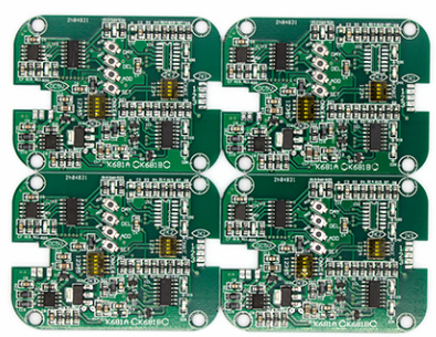
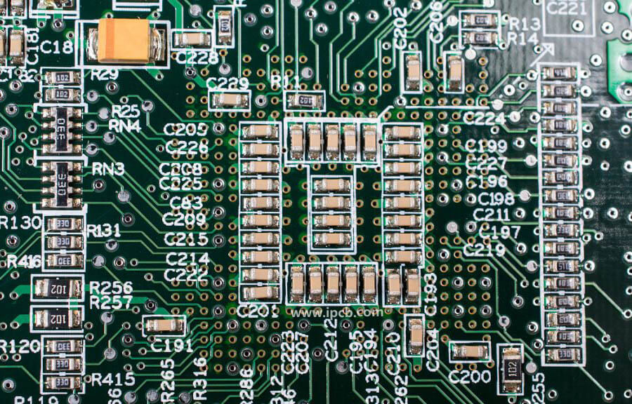
A Printed Circuit Board (PCB) is the foundation of modern electronic products. It provides mechanical support and electrical interconnection for electronic components while integrating conductive circuits, pads, vias, and other structures into a compact platform.
In simple terms, a PCB is an insulating substrate on which conductive patterns are formed according to a predefined circuit design. These conductive patterns connect electronic components electrically and provide the required functions for signal transmission, power distribution, grounding, and circuit protection.
Today, PCB Manufacturing is essential to almost every electronic application, ranging from watches, smartphones, computers, and communication equipment to industrial controls, medical devices, automotive electronics, aerospace systems, and military equipment.
Without a reliable PCB, integrated circuits and other electronic components cannot be efficiently interconnected or securely assembled. A well-designed and properly manufactured PCB provides:
- Mechanical support for electronic components
- Electrical interconnection between components
- Signal transmission and power distribution
- Controlled impedance for high-speed applications
- Grounding and electromagnetic interference control
- Soldering and assembly support
- Component identification and maintenance information
For these reasons, PCB technology has become one of the most important foundations of modern electronics.
What Is PCB Manufacturing?
PCB Manufacturing refers to the complete process of converting PCB design data and raw materials into a finished circuit board. Depending on the PCB structure, material, layer count, circuit density, and performance requirements, different manufacturing technologies may be used.
A typical PCB Fabrication process can involve chemical, photochemical, electrochemical, mechanical, thermal, and computer-aided manufacturing technologies. Modern factories also use CAM systems to convert design data into manufacturing instructions and optimize production parameters.
PCB production is not a single process. It consists of multiple interconnected stages, including material preparation, drilling, circuit imaging, copper plating, etching, solder mask application, surface finishing, testing, inspection, and final packaging.
Because every process affects subsequent operations, strict process control is essential. A problem in drilling, registration, copper plating, etching, or solder mask application can affect the reliability and yield of the entire production batch.
Different Types of Printed Circuit Boards
The manufacturing process varies according to the structure and application of the PCB. Common types include flexible PCBs, rigid PCBs, rigid-flex PCBs, single-sided PCBs, double-sided PCBs, and Multilayer PCBs.
Flexible PCB
Flexible PCBs use flexible insulating materials, commonly polyimide, to provide electrical interconnection while allowing the circuit to bend or fold. They are widely used in smartphones, cameras, wearable devices, automotive electronics, medical equipment, and compact electronic products.
Rigid PCB
A Rigid PCB uses a solid substrate that maintains its physical shape during operation. FR-4 is one of the most widely used materials for rigid circuit boards because of its good electrical insulation, mechanical strength, thermal performance, and cost efficiency.
Single-Sided PCB
A single-sided PCB contains conductive circuitry primarily on one side of the substrate. It has a relatively simple structure and is commonly used in cost-sensitive electronic products and applications with lower circuit density.
Double-Sided PCB
A double-sided PCB has copper circuitry on both sides of the insulating substrate. Through-hole technology and plated through holes are commonly used to electrically connect the two sides.
Compared with single-sided boards, double-sided PCBs provide greater routing flexibility and higher circuit density.
Multilayer PCB
A Multilayer PCB consists of multiple copper layers separated by insulating dielectric materials. Internal signal, power, and ground layers can be interconnected through plated through holes, blind vias, buried vias, and other interconnection structures.
Multilayer technology enables much higher circuit density and is widely used in computers, networking equipment, industrial electronics, automotive systems, telecommunications, and high-performance electronic devices.
Typical PCB Manufacturing Process
Although the exact process varies according to PCB type and manufacturer capabilities, a typical PCB Manufacturing Process includes several major stages.
1. Material Preparation and Cutting
The process begins with copper-clad laminate or other specified PCB materials. The material is cut into panels according to the required production dimensions.
Material selection is important because the substrate directly affects the PCB’s electrical, thermal, mechanical, and reliability characteristics.
Common materials include FR-4, high-frequency laminates, high-Tg materials, polyimide, and other specialized dielectric materials.
2. Inner-Layer Circuit Fabrication
For multilayer boards, the inner-layer circuits are manufactured before lamination.
The typical process includes:
- Surface cleaning and preparation
- Dry film lamination
- Circuit imaging
- Exposure
- Development
- Copper etching
- Dry film stripping
- Inspection
Advanced imaging technologies can provide greater circuit accuracy for fine-line and high-density applications.
3. Drilling
Drilling creates holes required for component installation and electrical interconnection.
Depending on the PCB structure, manufacturers may use mechanical drilling or laser drilling. Mechanical drilling is commonly used for through holes, while laser drilling is widely used for microvias in HDI applications.
Drilling accuracy is critical because hole position directly affects layer-to-layer registration and subsequent copper plating.
4. Through-Hole Metallization
After drilling, the exposed hole walls are not electrically conductive because they consist primarily of resin and glass-fiber materials.
A chemical pretreatment process is therefore used to prepare the hole walls, followed by electroless copper deposition. This creates a conductive copper layer inside the holes.
Electroplating is then used to increase copper thickness and improve the reliability of the interconnection.
5. Lamination
For a Multilayer PCB, the processed inner layers are stacked together with prepreg and copper foil according to the specified stack-up design.
The stack is laminated under controlled temperature and pressure. During this process, the resin flows and cures, bonding the different layers into a single rigid structure.
Lamination quality has a significant influence on:
- Layer registration
- Dielectric thickness
- Interlayer adhesion
- Thermal reliability
- Electrical performance
- Overall PCB reliability
6. Outer-Layer Circuit Formation
After lamination and drilling, the outer-layer circuitry is fabricated.
The process may include dry film application, imaging, development, copper pattern plating, tin plating, etching, and stripping.
The objective is to accurately form the required traces, pads, and other conductive structures while maintaining the specified line width and spacing.
7. Solder Mask Application
Solder mask is applied to protect exposed copper and prevent unwanted solder bridges during component assembly.
Green is the most common solder mask color, although black, blue, yellow, red, and other colors are also available.
The solder mask provides several important functions:
- Prevents solder bridging
- Protects copper from oxidation
- Improves electrical insulation
- Provides mechanical and environmental protection
- Defines exposed solderable areas such as pads
High-precision PCB production commonly uses photosensitive solder mask technology to achieve accurate openings around fine-pitch pads.
8. Surface Finishing
Exposed copper pads require a suitable surface finish to improve solderability, protect the copper surface, and meet application-specific reliability requirements.
Common surface finishes include:
- HASL
- Lead-free HASL
- ENIG
- ENEPIG
- OSP
- Immersion tin
- Immersion silver
The appropriate surface finish depends on factors such as component pitch, assembly process, shelf life, electrical requirements, and cost.
9. Silkscreen and Identification
Silkscreen is used to print reference designators, component markings, polarity indicators, logos, and other identification information.
Clear markings can simplify PCB assembly, inspection, troubleshooting, and maintenance.
10. PCB Testing and Inspection
Testing is a critical part of PCB Fabrication because manufacturing defects may not always be visible during visual inspection.
Depending on the product requirements, manufacturers may use:
- Automated Optical Inspection (AOI)
- Electrical testing
- Flying probe testing
- X-ray inspection
- Dimensional inspection
- Cross-sectional analysis
- Solderability testing
- Reliability testing
Electrical testing verifies whether the intended circuits are properly connected and whether unwanted open or short circuits are present.
PCB Assembly and Surface Mount Technology
After PCB fabrication is completed, the boards may proceed to PCB assembly.
Surface Mount Technology (SMT) has become one of the most important assembly technologies because it enables electronic components to be mounted directly onto PCB pads without requiring traditional through-hole leads for every component.
A typical SMT process includes:
- Solder paste printing
- Solder paste inspection
- Component placement
- Reflow soldering
- AOI inspection
- X-ray inspection when required
- Functional or electrical testing
Compared with traditional through-hole assembly, Surface Mount Technology provides higher component density, shorter electrical connections, improved automation, and better suitability for compact electronic products.
Why PCB Manufacturing Process Control Matters
A modern PCB Manufacturing Process contains many interconnected steps. The quality of the final board depends not only on individual processes but also on how accurately those processes work together.
Important control points include:
- Line width and spacing
- Layer-to-layer registration
- Hole position accuracy
- Copper thickness
- Via reliability
- Lamination parameters
- Solder mask registration
- Surface finish quality
- Electrical performance
- Final inspection
As electronic products become smaller and more powerful, PCB manufacturers must continuously improve manufacturing precision.
Fine-line circuits, microvias, high-density interconnections, advanced substrates, and complex multilayer structures require more accurate equipment and stricter process control.
The Evolution of PCB Manufacturing Technology
PCB technology has evolved from relatively simple single-sided boards to highly complex HDI and high-layer-count structures.
Traditional PCB production mainly relied on subtractive copper etching. However, increasing circuit density has created greater demand for advanced technologies such as laser drilling, laser direct imaging, sequential lamination, microvia formation, advanced copper plating, and modified semi-additive processes.
At the same time, high-speed and high-frequency applications require tighter control of:
- Trace impedance
- Dielectric thickness
- Copper roughness
- Signal integrity
- Power integrity
- Crosstalk
- Return-current paths
Therefore, modern PCB Manufacturing is no longer limited to producing conductive patterns. It must also support the electrical, thermal, mechanical, and reliability requirements of increasingly sophisticated electronic systems.
Kingda’s PCB Manufacturing Capabilities
Kingda focuses on providing reliable PCB manufacturing solutions for a wide range of electronic applications.
By integrating engineering support, manufacturing process control, inspection, and quality management, Kingda can support different PCB requirements ranging from conventional rigid boards to high-density and complex multilayer designs.
For customers with demanding PCB requirements, selecting an experienced manufacturer is important because manufacturing capability directly influences yield, consistency, delivery, and long-term product reliability.
Conclusion
The development of electronic technology continues to drive PCB manufacturing toward higher density, smaller geometries, greater layer counts, improved reliability, and more sophisticated materials.
From single-sided and double-sided boards to advanced Multilayer PCB structures, every stage of production requires accurate process control and professional engineering experience.
A complete PCB Manufacturing Process typically involves material preparation, circuit fabrication, drilling, plating, lamination, etching, solder mask application, surface finishing, inspection, and electrical testing. When PCB assembly is required, Surface Mount Technology further enables high-density and automated electronic manufacturing.
As a professional PCB manufacturer, Kingda continues to improve manufacturing technologies and quality control systems to provide reliable PCB solutions for modern electronic products.