PCB Manufacturing Process: A Complete Guide to PCB Production
Printed circuit boards are essential components in almost every modern electronic product. From consumer electronics and industrial control systems to automotive electronics, telecommunications equipment, and medical devices, PCBs provide the electrical connections and mechanical foundation required for reliable electronic operation.
As electronic products become smaller, faster, and more highly integrated, the requirements for PCB Manufacturing continue to increase. Modern PCB manufacturers must deliver not only stable production quality but also tighter tolerances, higher circuit density, advanced interconnection technologies, and faster delivery.
Understanding the complete PCB Manufacturing Process can help engineers, purchasing teams, and product developers select appropriate manufacturing technologies and make better design decisions before production begins.
PCB manufacturing is a multi-stage industrial process used to transform PCB design data and raw materials into finished printed circuit boards.
Depending on the board type and application, the manufacturing process may include:
The exact process depends on the PCB structure, number of layers, material, circuit density, hole technology, surface finish, and application requirements.
For companies looking for an integrated manufacturing partner, professional PCB Fabrication capabilities can help connect PCB design requirements with actual production processes and improve manufacturability.
The first step in PCB Production is selecting and preparing the appropriate raw materials.
The substrate provides the mechanical structure of the circuit board, while copper foil forms the conductive circuitry. Different applications require different combinations of substrate materials, copper thicknesses, and dielectric characteristics.
FR-4 is one of the most commonly used PCB substrate materials because of its balanced electrical, mechanical, thermal, and cost characteristics.
It is suitable for a wide range of consumer electronics, industrial equipment, control systems, communication products, and general electronic applications.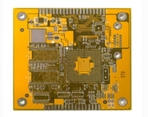
For demanding high-frequency or high-speed applications, however, specialized laminate materials may be required to achieve the necessary dielectric properties and signal integrity.
High-frequency and high-speed circuits can be sensitive to dielectric constant, dissipation factor, copper roughness, and material consistency.
Specialized laminate materials may therefore be used to reduce signal loss and improve electrical performance at higher frequencies.
Material selection should be based on actual electrical, thermal, mechanical, and environmental requirements rather than simply choosing the most advanced material available.
Multilayer PCB production begins with the fabrication of the inner copper layers.
The copper surface is cleaned and prepared before a photosensitive material is applied. The circuit pattern is then transferred onto the board through an imaging process.
The exposed areas are developed, and unwanted copper is removed through controlled chemical etching.
The result is a precisely defined copper circuit pattern representing the electrical connections inside the multilayer PCB.
Accurate imaging and etching are particularly important for fine-line designs. As trace width and spacing become smaller, manufacturing tolerances become tighter and process control becomes more demanding.
For multilayer PCBs, individual circuit layers must be combined into a single rigid structure.
The inner circuit layers are stacked together with dielectric materials and copper foils according to the specified layer stack-up.
Heat and pressure are applied during the lamination process to bond the layers together.
Layer alignment is critical during this stage. Even small registration errors can affect via connections, trace geometry, impedance characteristics, and overall board reliability.
For high-layer-count and high-density designs, precise lamination control is essential to achieving consistent PCB performance.
Drilling creates the holes required for component mounting and electrical interconnection.
Conventional PCBs commonly use mechanical drilling to create through-holes. More advanced PCB structures may require laser drilling for microvias and other high-density interconnection technologies.
The drilling process must control several parameters, including:
Small holes and high-density via structures require more precise equipment and tighter process controls.
For HDI boards, laser-drilled microvias can help designers create compact interconnections and increase routing density without significantly increasing board dimensions.
After drilling, the exposed hole walls must be prepared for metallization.
A conductive copper layer is deposited onto the hole walls so that electrical connections can be established between different PCB layers.
Additional copper plating can then increase the required copper thickness and improve electrical and mechanical reliability.
Uniform plating is particularly important for boards with demanding current-carrying requirements, small vias, and high aspect-ratio holes.
Poor plating control can result in insufficient copper thickness, voids, cracks, or unreliable electrical connections.
The outer copper layers are processed to create the final visible circuit patterns.
Similar imaging, developing, etching, and plating processes are used to define the required traces, pads, and other conductive structures.
At this stage, manufacturing accuracy directly affects trace width, spacing, pad dimensions, and solderability.
Fine-line PCB designs require particularly strict control because small variations can affect electrical performance and manufacturing yield.
As electronic products become smaller and more powerful, conventional PCB structures are increasingly complemented by advanced manufacturing technologies.
High-density interconnect technology allows manufacturers to create compact circuit structures using microvias, blind vias, buried vias, and fine-line routing.
HDI technology is widely used when designers need more routing capacity within a limited board area.
The manufacturing process can involve laser drilling, sequential lamination, fine-line imaging, precision plating, and multiple inspection stages.
These additional processes make HDI production more complex than conventional multilayer PCB fabrication.
High-speed electronic systems require careful control of signal transmission characteristics.
PCB manufacturing must consider material properties, stack-up design, trace geometry, impedance, dielectric thickness, copper characteristics, and manufacturing tolerances.
In high-speed applications, even relatively small variations in manufacturing parameters can affect signal integrity.
For this reason, high-frequency and high-speed PCB production requires close coordination between PCB design and manufacturing engineering.
Flexible and rigid-flexible PCBs can provide advantages where space, weight, bending, or three-dimensional packaging is important.
These boards require specialized materials and manufacturing processes compared with conventional rigid FR-4 PCBs.
They are commonly used in compact electronic products, medical equipment, automotive systems, aerospace electronics, and other applications where conventional rigid boards may be difficult to integrate.
In addition to standard PCB fabrication, many applications require specialized processes to achieve specific electrical, thermal, or mechanical performance.
Heavy copper technology increases the copper thickness of selected PCB layers.
This can improve current-carrying capacity and thermal performance, making heavy copper PCBs suitable for power electronics, industrial control equipment, automotive systems, and other high-current applications.
Resin plugging is used to fill selected PCB vias with resin.
This process can help prevent solder from flowing into certain holes during assembly and can support applications requiring controlled via structures or improved surface flatness.
Plated half-holes are commonly used for module-to-board connections and edge-mounted electronic assemblies.
The plated structure provides an electrical interface while allowing the PCB to be directly connected to another board or module.
Mechanical PCB requirements may include counterbored or countersunk holes to accommodate specific fasteners.
These structures are particularly useful when PCB assemblies need to be mechanically integrated into housings or equipment.
After circuit fabrication, a solder mask is applied to protect exposed copper areas and reduce the risk of accidental solder bridging during assembly.
The solder mask also provides electrical insulation and helps protect the PCB surface from environmental contamination.
Different solder mask colors may be available depending on the manufacturer’s process and customer requirements.
Silkscreen printing is then used to add reference designators, component identifiers, logos, polarity indicators, warning marks, and other information to the PCB surface.
Clear and accurate silkscreen markings can make PCB assembly, inspection, maintenance, and troubleshooting easier.
Surface finishing protects exposed copper pads and improves solderability.
Common PCB surface finishes include:
The appropriate surface finish depends on factors such as component package type, soldering process, storage requirements, electrical performance, environmental conditions, and product lifetime.
For fine-pitch components and demanding assembly applications, a more controlled surface finish may be preferred to achieve consistent soldering performance.
Quality inspection is an essential part of the PCB Manufacturing Process.
Manufacturers may use automated optical inspection, dimensional inspection, electrical testing, X-ray inspection, and other quality-control methods depending on board complexity and customer requirements.
Typical inspection items include:
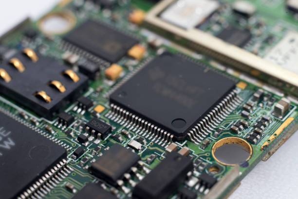
Electrical testing can identify open circuits and short circuits that may not be visible during visual inspection.
For high-reliability applications, additional testing and documentation may be required to verify that the finished PCB meets specified performance and quality requirements.
Production efficiency has become increasingly important as electronics companies shorten product development cycles.
For engineering teams, rapid prototype production allows PCB designs to be physically tested before moving into larger-scale manufacturing. This can help identify electrical, mechanical, and manufacturing problems at an earlier stage.
For low-volume products, flexible production capacity can reduce inventory pressure while allowing companies to respond more quickly to changing market requirements.
For larger production volumes, stable process control and efficient manufacturing scheduling become critical for maintaining consistent quality and delivery performance.
A capable manufacturer should therefore combine equipment, engineering expertise, quality management, production planning, and supply-chain coordination rather than focusing solely on individual manufacturing processes.
PCB fabrication produces the bare circuit board, but many electronic products require additional assembly processes before the final product can be tested and used.
PCB Assembly may include component procurement, solder paste printing, SMT component placement, reflow soldering, through-hole assembly, inspection, testing, and final packaging.
The relationship between PCB fabrication and assembly is important because a board that is technically manufacturable may still create assembly problems if pad dimensions, component spacing, solder mask openings, or other design parameters are not properly optimized.
For this reason, PCB manufacturers and assembly providers should consider manufacturability and assembly requirements as early as possible in the product development process.
Companies can improve manufacturing efficiency by optimizing the PCB design before production begins.
Use a layer structure that provides the required routing capacity and electrical performance without adding unnecessary layers.
A well-designed stack-up can reduce material usage and simplify manufacturing.
Trace width, spacing, hole diameter, via structures, copper thickness, and board tolerances should be selected according to realistic manufacturing capabilities.
Designing outside standard manufacturing capabilities can increase production difficulty and reduce yield.
PCB design should account for the subsequent assembly process.
Component spacing, pad geometry, solder mask openings, fiducials, thermal pads, and other features can affect SMT and through-hole assembly quality.
Design for Manufacturing review can identify potential problems before the PCB enters production.
A DFM review may examine circuit spacing, hole sizes, layer stack-up, copper distribution, board dimensions, surface finish, and assembly-related design features.
Resolving these issues before fabrication can reduce rework, delays, and unnecessary manufacturing expenses.
A typical electronics development cycle may begin with PCB design and prototype fabrication before progressing to low-volume and high-volume production.
Prototype manufacturing allows engineers to validate the initial design and identify potential problems.
Once the design is verified, production quantities can be increased according to market demand.
This approach allows companies to reduce development risks while gradually optimizing production cost, manufacturing efficiency, and supply-chain stability.
For projects requiring both circuit-board production and assembly, an integrated manufacturing workflow can further simplify supplier management and reduce communication gaps between PCB fabrication and assembly processes.
Modern PCB Manufacturing is a complex process that combines materials engineering, circuit fabrication, drilling, plating, lamination, surface treatment, inspection, and quality management.
As electronic products move toward smaller dimensions, higher integration, faster signal speeds, and greater reliability, manufacturers must continuously improve their production technologies and process controls.
The right manufacturing strategy depends on the PCB’s layer count, material, circuit density, electrical requirements, mechanical structure, production volume, and end-use application.
Whether a project requires a simple two-layer board, a high-density HDI PCB, a high-frequency circuit board, a heavy-copper PCB, or a flexible and rigid-flex structure, selecting the appropriate PCB Fabrication process is essential for achieving consistent quality and reliable performance.
By combining DFM principles, appropriate material selection, optimized manufacturing processes, effective inspection, and professional assembly capabilities, electronics companies can shorten development cycles, reduce production risks, and build more reliable products.