PCB Manufacturing Process: A Complete Production Guide
A bare board leaves the factory only after dozens of controlled steps. Each step changes the copper, the laminate or the surface, and each one can spoil the work done before it. Engineers and buyers who understand the sequence ask sharper questions at quotation and first article. This guide walks the production flow from material selection to final test. It explains why each stage exists and what to verify before a lot is released.
The process changes with the board. Layer count, material, trace density, hole technology and surface finish all shift the route through the factory. A simple two-layer board may pass through the line in days, while a high-density multilayer build needs sequential lamination and extra inspection. Buyers should treat the process route as part of the quotation, not as a detail hidden behind a unit price. The same discipline applies to rapid PCBA prototyping, where early samples reveal process limits before volume begins.
Material and Stackup Choices
Production starts with the substrate and the copper foil. The laminate gives the board its mechanical strength and its dielectric behavior. The copper sets the current capacity and the etching resolution. Standard FR-4 covers most consumer, industrial and control products because its electrical, thermal and cost balance suits general work. High-speed and high-frequency designs may need specialized laminates with tighter dielectric constant and lower loss. Material choice should follow the real electrical and thermal requirement, not the most advanced datasheet available.
Copper weight matters as much as the resin system. Heavier copper helps current-carrying traces and thermal spreading, but it also demands longer etching and tighter process control. Thin copper supports fine lines but leaves less margin for plating variation. The stackup drawing should state copper weight per layer, dielectric thickness and the target impedance where relevant. A buyer should confirm that the quoted stackup matches the drawing before tooling starts. Small mismatches here become expensive rework later in the run.
Inner Layer Imaging and Etching
Multilayer production begins with the inner layers. The copper surface is cleaned so the photosensitive film bonds evenly. The circuit image is exposed, developed, and the unwanted copper is etched away. What remains is the conductor pattern for that layer. Fine-line designs push this step hardest, because trace width and spacing shrink while tolerance stays fixed. Imaging accuracy and etch control decide whether the finished trace meets the drawing. A drift in etch chemistry or conveyor speed shows up as a width error across the panel.
Etching is a balance between removing copper and protecting the trace. Over-etch narrows conductors and weakens current capacity. Under-etch leaves copper slivers that can bridge adjacent traces. The factory controls etchant strength, temperature and dwell time, then checks trace width on samples. Buyers reviewing a fine-line order should ask how trace width is verified and how often. That answer says more about capability than a machine list does. Documented measurement is the only reliable proof of process control.
Lamination and Layer Registration
The inner layers are stacked with prepreg and copper foil according to the approved stackup. Heat and pressure bond the package into one rigid structure. Registration is the critical variable. Each layer must align with the target position so that vias and traces connect as designed. Small offsets can shift impedance, reduce annular ring and weaken via reliability. High-layer-count boards leave less room for error, so the press cycle and the tooling holes must be tightly controlled. Alignment is checked before and after the press.
Lamination also controls dielectric thickness, which directly affects impedance. Resin flow depends on prepreg type, pressure profile and temperature ramp. A press cycle that runs too hot or too fast can leave voids or thin dielectric in places. The factory should record press parameters for each lot and keep them with the build record. When a repeat order arrives, those records show whether the same conditions were used. Consistency across lots is what makes a stackup predictable in the field.
Drilling and Hole Quality
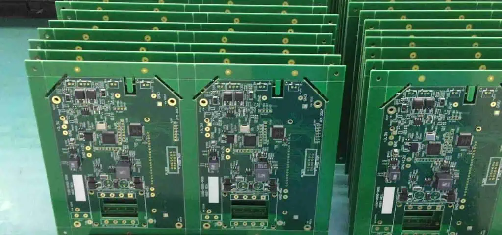
Drilling creates the holes for component leads and layer-to-layer connections. Mechanical drilling handles through-holes in conventional boards. Laser drilling forms microvias in high-density structures. Both processes must control hit accuracy, spindle speed, feed rate and bit wear. A worn bit smears the resin and leaves a rough wall that plating cannot cover reliably. Hole quality is checked by cross-section on samples. For dense builds, the drill program and the stackup must be reviewed together before the first panel is cut.
Aspect ratio is a practical limit worth watching. Compared with a shallow hole, plating a deep and narrow hole evenly is more difficult. When the ratio climbs, the factory needs better agitation, chemistry control and inspection. Buyers should confirm that the quoted hole sizes fall inside the supplier’s proven range. Pushing beyond that range adds risk without adding function. The drill chart and the stackup should agree on every hole before release. Any conflict between them is a question for the engineer, not a guess for the operator.
Plating and Copper Deposition
After drilling, the hole walls must be prepared for metallization. A thin conductive layer is deposited, then copper plating builds the wall to the required thickness. Uniform plating matters most for small vias, high aspect ratios and heavy current paths. Poor control leaves thin copper, voids or cracks that fail in the field. The plating line is monitored through chemical analysis and thickness measurement on coupons. Surface copper also grows during plating, so the outer layer pattern must account for the added thickness before etching.
Plating quality links directly to reliability. A via with a thin wall may pass a quick electrical test and still crack under thermal cycling. Factories that care about this measure wall thickness by cross-section and track the trend over time. Buyers can ask for that data on high-reliability orders. It is concrete evidence that the process is watched rather than assumed. The same logic applies to surface copper uniformity, which affects etching and impedance across the panel.
Outer Layers and Solder Mask
The outer layers are imaged, plated and etched to form the final traces, pads and test points. Accuracy here sets trace width, pad size and solderability. After circuit formation, a solder mask covers the board except at pads and openings. The mask protects copper from oxidation, reduces solder bridging and provides insulation. Mask thickness and cure must be controlled so that fine-pitch pads stay clean and openings stay sharp. A mask that bleeds onto pads creates assembly defects that appear much later, at the soldering stage.
Silkscreen printing adds reference designators, polarity marks and warning symbols. Clear legends speed assembly, inspection and repair. The legend must not sit on pads or block test points. Surface finish comes next and protects exposed copper while improving solderability. The choice depends on component pitch, storage time, soldering process and product life. Buyers should match the finish to the assembly plan rather than defaulting to one option. A finish that suits a long-stored board may be a poor fit for fine-pitch parts.
Electrical Test and Inspection
Inspection catches defects before shipment, and its greater value is the feedback it gives. Automated optical inspection checks pattern, mask and legend against the design data. X-ray inspection reveals hidden joints and via quality on dense boards. Electrical test confirms continuity and isolation across the netlist. Each method covers a different failure mode, so the test plan should match board complexity. A simple board needs less coverage than a dense multilayer build with fine features. The plan should be written down and agreed before production.
Test data also supports improvement. When a defect appears, the factory can trace it to a specific step and correct the cause. That closed loop lowers defect rates over time. Buyers should ask for test reports with each lot and review them against the drawing. A report that lists only pass or fail tells little. One that shows what was measured and where builds real confidence. This is also why PCBA testing planning belongs early in the project, before the first panel is built.
Assembly Interface and Verification
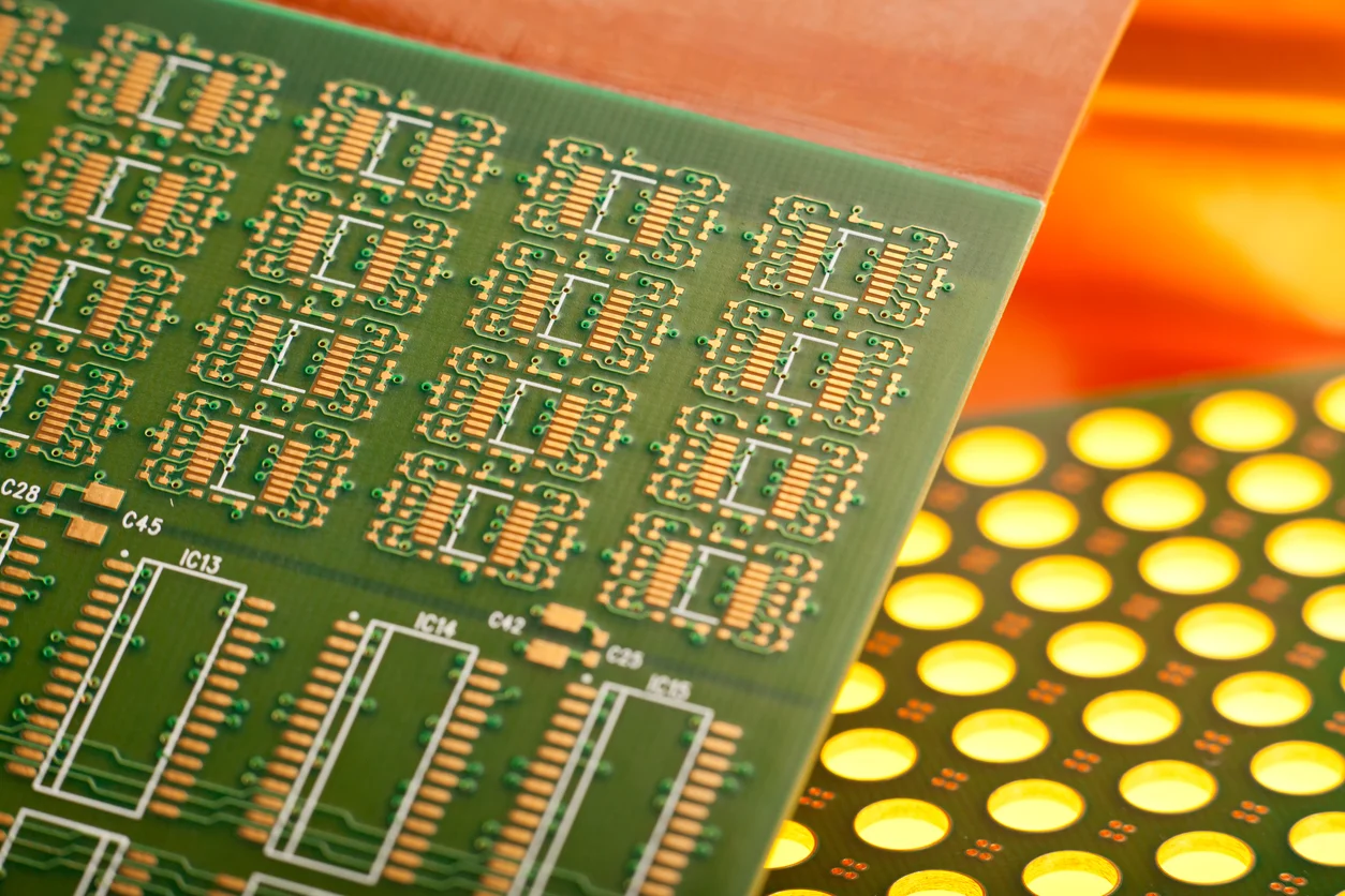
Fabrication ends with a bare board, but most products continue into assembly. Pad geometry, mask openings, fiducials and component spacing decide whether that next step runs smoothly. A board can pass fabrication and still cause assembly problems if these features are poorly defined. Design review before production is the cheapest place to catch them. The factory and the assembly house should work from the same drawing and the same revision. Any disagreement between them should be resolved before tooling, not after the first lot ships.
For projects that need both stages, an integrated flow reduces handoffs and miscommunication. Solder paste printing, component placement, reflow and inspection all depend on the bare board being right. When fabrication and SMT PCB assembly sit under one roof, questions about pad size or mask clearance reach the right engineer quickly. That speed matters on a tight schedule. Buyers comparing suppliers should ask how the two stages share data and who owns the final inspection record. Clear ownership prevents defects from falling between departments.
Repeat Orders and Process Records
A first article proves the process once. Repeat orders prove it can be repeated. Parameters drift, materials change and operators rotate, so the factory must record what ran and compare it with the approved setup. Material lots, press cycles, plating chemistry and test results all belong in the build record. If a field return shows up months later, that record provides the quickest path to the root cause. Buyers should treat documentation as part of the product, not as paperwork requested after a problem.
Prototypes are the cheapest place to learn. Early samples expose pad geometry issues, tolerance stack-ups and process behavior before large volumes are committed. A pilot run followed by a design review often shortens the path to volume. For buyers planning that route, turnkey PCB assembly can cover sourcing, build and test in one schedule. The goal is a process that produces the same result on Monday and on Friday. Repeatability, backed by records, is what separates a capable supplier from a lucky one.
The practical takeaway is simple. Ask for the stackup, the process route, the test plan and the build record before you place a volume order. Confirm that hole sizes, trace widths and finish choices sit inside the supplier’s proven range. Review the first article against the drawing, then compare the second lot with the first. A supplier that answers these questions with data is ready for your program. A supplier that responds with assurances instead of data is asking you to take on the risk.
Good PCB assembly starts with a bare board built to a documented, repeatable process.