PCB Assembly DFM: PCB Design, PCB Manufacturing & DFM Guide
Design for Manufacturability (DFM) is the process of reviewing and optimizing a PCB design so that it can be fabricated and assembled efficiently, consistently, and reliably.
DFM is one of the most valuable activities in the product-development process because manufacturing problems are generally much less expensive to correct during the design stage than after production has started.
A PCB may be electrically functional and still be difficult or expensive to manufacture. Issues involving component placement, pad geometry, solder mask, stencil design, vias, panelization, or inspection access can create production delays and quality problems if they are not identified early.
This guide explains the most important DFM considerations for PCB Assembly, what engineers should review before submitting manufacturing files, and what they should expect from a professional contract manufacturer’s DFM review.
Why Is DFM Important for Custom PCB Assembly?
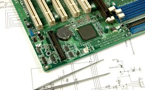
A successful PCB Design must satisfy more than electrical requirements. It should also be compatible with the fabrication, assembly, inspection, and testing processes used by the manufacturer.
A design that is difficult to manufacture may result in:
- First-article rework or redesign
- Lower production yield
- Increased inspection and troubleshooting time
- Soldering defects and assembly problems
- Delays caused by repeated engineering changes
- Higher manufacturing and assembly costs
- Defects escaping into subsequent testing or field applications
Resolving these issues before production protects both project schedules and budgets.
Early DFM collaboration also improves communication between engineering teams and contract manufacturers because both parties are working from a clearly defined and manufacturable design.
Key DFM Areas for PCB Assembly
1. Component Placement and Orientation
Component placement has a direct effect on automated assembly, soldering, inspection, and rework.
Components positioned too close to:
- The PCB edge
- Other components
- Mounting holes
- Mechanical keep-out areas
- Connectors
- Test points
may create manufacturing or inspection problems.
Engineers should verify the manufacturer’s recommended component-to-component and component-to-edge clearances before finalizing the layout.
Component orientation is also important.
Maintaining consistent orientation for polarized or orientation-sensitive components—such as electrolytic capacitors, diodes, LEDs, connectors, and ICs—can simplify automated inspection and reduce the risk of assembly errors.
However, orientation should also consider the requirements of the soldering process, component markings, and inspection equipment.
2. Pad Design and Footprints
Incorrect PCB footprints are among the most costly DFM problems because they can result in poor solder joints even when the component itself is correctly placed.
A pad that is too small may provide insufficient soldering area or reduce solder-joint reliability. Excessively large pads can increase solder volume and, for fine-pitch components, contribute to solder bridging.
Engineers should use manufacturer-recommended land patterns or appropriate IPC-based footprint guidance whenever possible.
Special attention should be given to:
- Fine-pitch QFPs
- QFNs
- BGAs
- Bottom-terminated components
- Small passive components
- Thermal pads
- Connector footprints
Custom footprints should be reviewed carefully before production.
A professional DFM review should identify unusual or potentially problematic pad geometries rather than simply checking whether the PCB can technically be manufactured.
3. Solder Mask and Stencil Design
Solder mask openings and stencil apertures have a direct effect on solder-paste deposition.
An excessively large solder-mask opening may reduce the defined pad area and affect solder-paste placement. On fine-pitch components, insufficient solder-mask webbing between adjacent pads can also create manufacturing challenges.
Stencil aperture design is equally important.
A stencil opening that is too large may deposit excessive solder paste, while an opening that is too small may produce insufficient solder volume.
For fine-pitch, BGA, QFN, and other challenging packages, stencil design may require:
- Aperture size optimization
- Aperture reduction
- Aperture segmentation
- Home-plate or other specialized aperture geometries
- Localized stencil thickness considerations
The exact approach depends on the component package, pad dimensions, solder-paste material, stencil technology, and assembly process.
4. Via Placement Relative to SMT Pads
Vias located directly inside or immediately adjacent to SMT pads can affect solder-joint formation.
An open via inside a pad may allow molten solder to flow into the via during reflow. This can reduce the amount of solder remaining on the pad and potentially affect joint quality.
This is commonly referred to as solder wicking or solder drainage.
Via-in-pad designs can still be used effectively, particularly for HDI, fine-pitch, BGA, and thermal applications, but the vias may require appropriate treatment such as:
- Via filling
- Via capping
- Controlled plating
- Other manufacturer-approved via-in-pad processes
If vias are required inside component pads for thermal or routing reasons, engineers should confirm the manufacturer’s recommended via treatment before releasing the design for production.
5. PCB Panelization
Panelization allows multiple PCB units to be processed together as a production panel.
It can improve manufacturing efficiency, particularly for smaller boards and higher-volume production, but panel design must be compatible with the assembly and depanelization processes.
Important panelization considerations include:
- V-score
- Tab routing
- Breakaway tabs
- Tooling rails
- Fiducial locations
- Tooling holes
- Component clearance from panel edges
- Board orientation
- Depanelization method
The location of components near the PCB edge is particularly important because mechanical stress during depanelization can affect sensitive components or solder joints.
If the customer supplies a pre-panelized PCB, the panel design should be reviewed with the manufacturer before production.
6. Fiducials and Assembly Markings
Fiducials provide optical reference points that help automated assembly equipment accurately determine PCB position and orientation.
Appropriate fiducial placement is particularly important for dense SMT assemblies and boards with fine-pitch components.
Assembly drawings and silkscreen markings should also be clear and consistent.
Useful documentation and markings may include:
- Reference designators
- Polarity indicators
- Pin-1 indicators
- Connector identification
- Component orientation marks
- Revision information
- Test-point identification
Clear markings reduce the risk of manual assembly errors and can make inspection and troubleshooting more efficient.
However, silkscreen should not overlap solder pads or interfere with critical manufacturing areas.
7. Component-to-Component and Component-to-Edge Clearance
Adequate spacing is necessary for automated placement, soldering, inspection, and rework.
The required clearance depends on:
- Component package
- Component height
- Soldering process
- Assembly equipment
- Inspection method
- Rework requirements
- PCB thickness
- Manufacturer capabilities
Large components placed close to small components can create shadowing or accessibility problems during inspection and rework.
Components positioned too close to the PCB edge may also interfere with panel rails or depanelization.
Therefore, engineers should not rely solely on generic clearance rules. The actual manufacturer’s DFM capabilities should be considered.
8. SMT and Through-Hole Interaction
Mixed-technology boards require additional DFM planning because SMT and through-hole components may be processed using different soldering methods.
A typical production sequence may involve:
SMT printing → SMT placement → reflow → through-hole insertion → wave or selective soldering → inspection and testing
However, the actual sequence depends on the PCB design.
When wave soldering is used, engineers must evaluate whether bottom-side SMT components can safely pass through the solder wave.
Selective soldering can provide greater process control when only specific through-hole locations need to be soldered.
Therefore, the decision between SMT, through-hole, and mixed technology should be considered during PCB Design, rather than after the design has been completed.
9. Testability and Test-Point Access
DFM should also include Design for Test (DFT) considerations.
A PCB that is easy to assemble but difficult to test can create production bottlenecks.
Engineers should consider:
- Test-point locations
- Test-point spacing
- Probe accessibility
- Ground test points
- Programming interfaces
- ICT requirements
- Flying-probe access
- Functional test requirements
Test points should be positioned so that the selected testing equipment can reliably access them without interfering with components or mechanical structures.
Early communication with the manufacturer is especially important if ICT or a dedicated test fixture will be used.
10. PCB Materials, Stackup, and Manufacturing Requirements
DFM is not limited to component assembly.
The underlying PCB fabrication requirements can also influence manufacturability and cost.
Important factors include:
- PCB layer count
- Laminate material
- Tg requirements
- Board thickness
- Copper thickness
- Trace width and spacing
- Controlled impedance
- Via structure
- Surface finish
- Solder mask requirements
For example, a multilayer HDI PCB with microvias and fine-line routing requires a more advanced fabrication process than a conventional two-layer FR-4 board.
These fabrication requirements should therefore be reviewed together with the assembly requirements.
What Should You Expect From a Professional DFM Review?
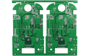
A meaningful DFM review should provide specific and actionable feedback.
Depending on the project, a manufacturer’s review may cover:
- Component placement
- Component clearances
- PCB edge clearances
- Footprints and pad geometry
- Solder-mask openings
- Stencil requirements
- Via-in-pad structures
- Panelization
- Fiducials
- Test-point accessibility
- SMT and through-hole process compatibility
- Material and stackup requirements
- Manufacturing tolerances
The feedback should explain what the problem is, why it matters, and what modification is recommended.
A useful DFM review should not simply provide a generic checklist or ask whether the designer has read a particular IPC standard. The purpose of DFM is to evaluate the actual design against real manufacturing processes and capabilities.
DFM and PCB Assembly Cost
Many factors that affect PCB Assembly Cost can be addressed during DFM.
For example:
- Reducing unnecessary component variety can simplify procurement and assembly.
- Standardizing component packages can improve production efficiency.
- Avoiding unnecessarily tight tolerances can reduce fabrication cost.
- Optimizing panelization can improve material utilization.
- Minimizing unnecessary through-hole operations can simplify assembly.
- Improving test-point accessibility can reduce testing complexity.
- Optimizing footprints and stencil apertures can improve soldering yield.
However, cost reduction should never be based solely on minimizing manufacturing steps.
A design change that reduces assembly cost but negatively affects thermal performance, reliability, electrical performance, or serviceability may increase the total product cost over its lifecycle.
The goal of DFM is therefore to find the most practical balance between PCB Manufacturing efficiency, quality, reliability, and cost.
DFM Checklist Before Sending PCB Files to a Manufacturer
Before submitting a design for production, engineers can use the following checklist:
PCB Design
- Board dimensions and mechanical outline are finalized.
- Layer stackup has been reviewed.
- Trace width and spacing meet manufacturing requirements.
- Via structures are appropriate for the selected fabrication process.
- Copper thickness is defined.
- Surface finish is specified.
Component Placement
- Component-to-component clearance has been checked.
- Component-to-edge clearance has been checked.
- Polarity and orientation are clearly defined.
- Mechanically sensitive components are appropriately supported.
- Fine-pitch components have adequate inspection and rework access.
SMT Assembly
- Component footprints have been verified.
- Pad dimensions are appropriate.
- Solder-mask openings have been reviewed.
- Stencil requirements have been considered.
- Via-in-pad structures have been reviewed.
- Fiducials are correctly positioned.
Through-Hole Assembly
- Hole sizes match component leads.
- Through-hole pad sizes are appropriate.
- Component spacing supports the selected soldering process.
- Wave or selective soldering requirements have been reviewed.
Testing
- Test points are accessible.
- Programming requirements are defined.
- ICT, flying-probe, or functional testing requirements are documented.
- Test fixtures are considered where necessary.
Manufacturing Documentation
- Gerber or equivalent fabrication files are complete.
- Drill files are included.
- BOM is complete and current.
- Pick-and-place data is available.
- Assembly drawings are included.
- Revision information is consistent across all files.
How Kingda Can Support PCB DFM
For a custom PCB Assembly project, early DFM communication can help identify manufacturing risks before fabrication and assembly begin.
Kingda can work from the customer’s PCB design and manufacturing documentation to evaluate key areas such as component placement, assembly process requirements, fabrication specifications, and production considerations.
For complex boards, providing the complete manufacturing package—including Gerber files, BOM, pick-and-place data, assembly drawings, stackup information, and testing requirements—allows the manufacturing team to conduct a more meaningful review.
The specific DFM recommendations and manufacturing limits should always be confirmed against the actual production process and equipment used for the project.
Conclusion
Design for Manufacturability (DFM) is an essential part of modern PCB Design and PCB Manufacturing. A circuit can be electrically correct and still create unnecessary manufacturing costs, yield problems, assembly defects, or production delays if manufacturability is not considered.
The most important DFM areas for PCB assembly include component placement, footprints, solder-mask openings, stencil design, via placement, panelization, fiducials, testability, and SMT/through-hole process compatibility.
The earlier these issues are identified, the easier they are to correct. By incorporating DFM into the design process and working with the manufacturer before production, engineers can develop PCB assemblies that are easier to fabricate, assemble, inspect, and test while maintaining the required performance and reliability.