Package on Package Design Guide
Package on package places a memory device on top of a logic device and connects the two through a ring of solder joints around the edge of the lower package. The arrangement saves board area and shortens the connection between the processor and its memory, and it concentrates a difficult set of mechanical problems into a single assembly step rather than spreading them across the board. The reward is a compact subsystem; the price is a narrow process window that has to be understood before the design is frozen.
How the Stack Is Built
The lower package carries a perimeter array of pads on its top surface. The upper package carries a matching array on its underside, and the two are joined by solder balls that are reflowed after the lower device has been attached to the board.
In the common flow, the bottom package is placed and reflowed first, then the top package is placed on the paste or on the flux that has been deposited on the bottom package pads, and the assembly passes through the oven a second time. Some processes attach both at once, which is faster but leaves less room to correct a placement error.
The interposer, when one is used, sits between the two devices and redistributes the connections. It allows a fine pitch die to be brought out to a coarser perimeter array, and it adds a layer of thermal expansion mismatch that has to be accounted for in the design of the joints.
Stack Height and Clearance
Stack height is the sum of the top package, the ball that joins the two packages, the bottom package and the ball that joins the bottom package to the board. It is bounded by the enclosure, and every element in the sum is a tolerance that has to be added rather than a nominal value.
The clearance under the top package is what limits the height of the components placed on the bottom package and the amount of underfill that can be applied. Where the gap is small, the underfill has to flow through a narrow channel, and the filler particle size becomes a design constraint rather than a process detail.
A warped package changes the effective stand off at the corners, so the clearance should be evaluated with the worst case warpage rather than with the room temperature shape. A design that just fits at room temperature will touch at reflow temperature, where the package is at its flattest but the board is not.
Warpage and Coplanarity
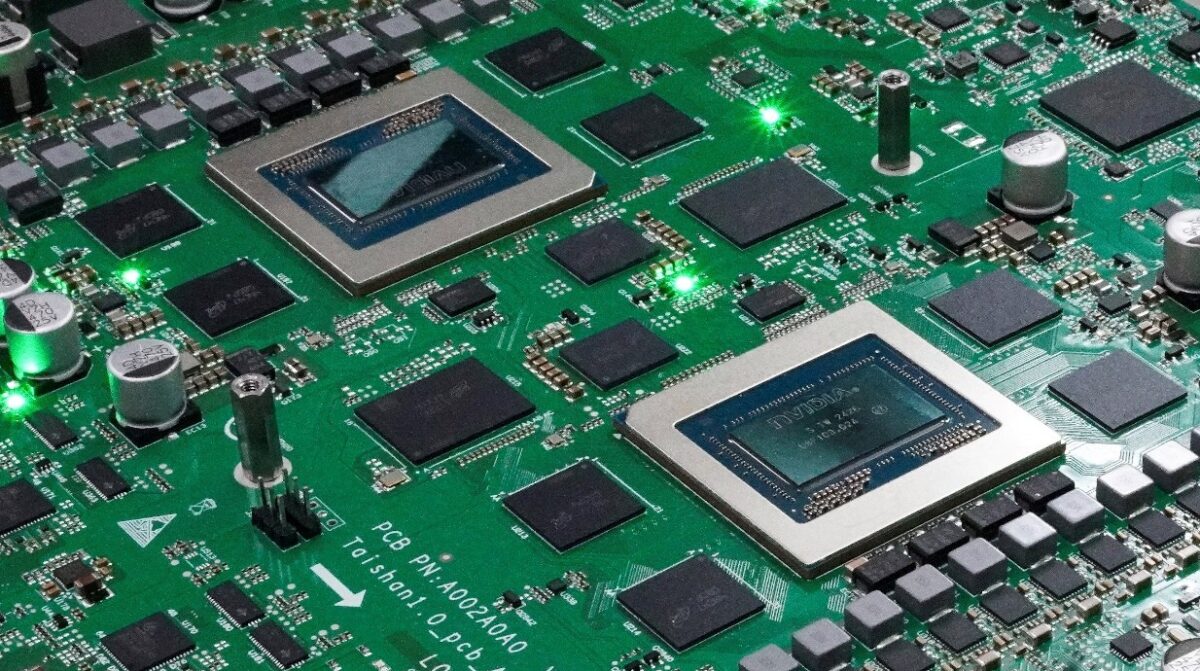
Warpage is the property that makes package on package difficult. The bottom package is thin, and it deforms as it passes through the reflow profile, so the pad ring that was coplanar at room temperature takes on a curved shape at the moment the solder is molten.
The two packages often warp in opposite senses, which is why a joint that opens at one corner during reflow is a common failure. The design response is to keep the ball diameter large enough to absorb a given displacement and to place the balls so that the distance between them is limited relative to the expected warpage.
Controlling warpage is a matter of package construction and of moisture. A package that has absorbed moisture will deform more as the water is released, so the storage and the bake before assembly are part of the warpage control rather than a separate step.
Materials and Solder Joints
The solder that joins the packages is often a different alloy from the one used on the board, chosen for a lower melting point so that the second reflow does not remelt the first. Where the same alloy is used twice, the process window depends on the thermal mass and on the order of assembly.
The solder joint in a stack is short and stiff, and it sees the full differential expansion between two packages that may have different bodies and different fillers. A slightly taller joint with a larger diameter reduces the strain per unit length, which is why the stand off is a reliability parameter and not just a height.
The surface finish on the bottom package pads must be compatible with the paste and the alloy, and it must survive the first reflow unchanged. A finish that oxidises during the first pass gives a poor second joint, and the defect appears at the top of the stack rather than at the board.
Placement, Reflow and Inspection
Placement accuracy is critical because the joint is held in position by surface tension that has a limited ability to pull a misaligned package into place. The vision system has to see the perimeter balls rather than the body, and the fiducial arrangement must allow that.
The reflow profile has to be gentle enough for the top package and hot enough for the bottom joint. The two requirements pull in opposite directions, and the profile is usually established for the largest and thinnest combination in the product family and then verified on the others.
Inspection of the stack is limited to X ray, which sees the joints through the package, and to a side view that shows the outer row. Both methods need a reference image from a known good assembly to be read quickly. The interior joints of a large array cannot be examined optically, so the process control relies on the placement data, the reflow profile and a periodic cross section.
Design Rules That Help
Keep the ball count as low as the routing allows, space the perimeter balls as far apart as possible, and avoid placing large components close to the bottom package where they increase the local thermal mass. A uniform thermal mass across the assembly gives a more even reflow.
Provide a keep out around the stack for the nozzle of the underfill dispenser and for the rework tool. Where rework is expected, the design should allow the top package to be removed without disturbing the bottom one, which usually means a different alloy or a controlled heat application.
Document the stack height with tolerances on the assembly drawing and include the warpage limit, the alloy and the underfill in the specification. Those four items are what allow the assembly house to build the stack the same way twice.
Practical Rules
Design the joints for the warpage, not for the nominal planar case, and verify the stack height against the enclosure using worst case tolerances. Keep the thermal mass uniform and leave room for the dispense and rework tools.
Record the alloy, the profile and the inspection results with the build records and the X ray inspection data, and review the derating assumptions whenever the stack height changes.
FAQ
Why is warpage the main problem in package on package? The thin bottom package deforms during reflow, so the pad ring is no longer planar when the solder is molten. Joints at the corners can open while the material is still liquid.
Why use a different alloy for the second reflow? A lower melting point alloy lets the top package be attached without remelting the joints that hold the bottom package to the board.
How is a stacked assembly inspected? X ray sees the joints through the package and a side view shows the outer row. Interior joints of a large array rely on process control and a periodic cross section.