PCB Prototype Assembly: Process, Types, Testing, Design Considerations, and Benefits
In today’s rapidly evolving electronics industry, manufacturers are under constant pressure to introduce products with more advanced features, smaller form factors, higher performance, and greater reliability. Developing and manufacturing a new electronic product or PCB design is a complex process that requires significant investment in engineering, materials, equipment, and production resources.
Even a minor design error or an unexpected manufacturing issue can lead to costly rework, production delays, or even an entire batch being rejected. To minimize these risks, manufacturers commonly use PCB prototype assembly before moving into mass production. A prototype allows engineers to evaluate the actual product, identify hidden design issues, validate component selection, and optimize the manufacturing process under real operating conditions.
As electronic devices become increasingly compact and sophisticated, prototype development has become an essential stage in modern electronics manufacturing. A well-designed PCB Prototype can serve as a bridge between an engineering concept and a production-ready product.
This guide explains the fundamentals of PCB Prototype Assembly, including its types, assembly process, materials and components, design considerations, testing methods, benefits, applications, common challenges, and key factors to consider when selecting a prototype assembly partner.
What Is PCB Prototype Assembly?
PCB Prototype Assembly is the process of mounting and soldering electronic components onto a printed circuit board before a product enters full-scale production. Engineers typically manufacture and assemble a limited number of prototype boards to evaluate the design’s functionality, manufacturability, electrical performance, mechanical compatibility, and overall reliability.
Unlike mass production, prototype assembly involves a relatively small quantity of boards. However, the fundamental manufacturing processes are generally similar to those used for production assemblies. Depending on the product, a prototype may involve SMT Assembly, through-hole assembly, or a combination of both.
The primary purpose of prototype assembly is to identify and resolve potential problems before they become expensive production issues. Engineers can evaluate:
- Electrical and functional performance
- Component compatibility
- PCB layout and routing
- Mechanical fit
- Soldering quality
- Thermal performance
- Signal integrity
- Manufacturing feasibility
- Assembly time and cost
- Product reliability under actual operating conditions
By identifying problems at an early stage, manufacturers can make design changes before committing to expensive tooling, component purchases, and large-scale production.
Types of PCB Prototype Assembly

The appropriate prototype assembly method depends on PCB complexity, component types, production requirements, budget, and testing objectives. The three common approaches are PTH Assembly, SMT Assembly, and mixed or hybrid PCB assembly.
1. PTH Prototype Assembly
PTH Assembly (Plated Through-Hole Assembly) is one of the traditional methods used for PCB assembly. Through-hole components have leads that pass through drilled holes in the PCB and are soldered to pads on the opposite side.
PTH assembly remains useful when a prototype contains:
- Large connectors
- Transformers
- Power components
- Mechanical switches
- High-current components
- Components requiring additional mechanical strength
Because through-hole components generally occupy more PCB space than surface-mount components, PTH assembly is less suitable for highly compact electronic products. Nevertheless, it remains valuable for power electronics, industrial equipment, and applications requiring strong mechanical connections.
2. SMT Prototype Assembly
SMT Assembly uses surface-mount devices (SMDs) that are placed directly onto copper pads on the PCB surface. SMT is the preferred approach for most modern electronic products because it supports compact layouts, high component density, and automated assembly.
During an SMT prototype build, solder paste is applied to the PCB using a stencil, followed by automated component placement and reflow soldering.
SMT prototype assembly is particularly suitable for:
- Smartphones and consumer electronics
- IoT devices
- Wireless modules
- Embedded systems
- Medical electronics
- Automotive electronics
- High-speed digital products
Because the same fundamental process can be transferred to mass production, SMT prototype assembly also provides valuable information about production readiness.
3. Hybrid PCB Prototype Assembly
A hybrid prototype combines SMT and PTH components on the same PCB. This approach is common when a design contains both compact integrated circuits and mechanically robust components such as connectors, switches, transformers, or power devices.
A hybrid PCBA can be tested under actual operating conditions to identify electrical, mechanical, thermal, and assembly-related problems before production.
PCB Prototype Assembly Process
Although prototype production involves a smaller quantity than mass production, a professional prototype assembly process should follow controlled manufacturing procedures. This helps ensure that prototype results accurately represent future production performance.
Design Review and Component Selection
The process begins with a comprehensive engineering review. The customer typically provides the PCB design files, Gerber or ODB++ data, schematic information, bill of materials (BOM), pick-and-place files, assembly drawings, and other manufacturing documentation.
The manufacturer reviews these files to identify potential problems before fabrication or assembly begins.
The review may include:
- PCB layer stack-up
- Component footprints
- Pad geometry
- Trace widths and spacing
- Component availability
- Polarity markings
- Assembly orientation
- BOM accuracy
- Manufacturing tolerances
- Thermal requirements
- DFM considerations
Component availability is especially important during prototype development. Using standard, readily available components can reduce procurement delays and make subsequent production easier.
PCB and Component Preparation
After the design is approved, the bare PCB and required components are prepared.
For SMT assembly, a solder paste stencil is normally produced according to the PCB pad pattern. Solder paste is then deposited onto the appropriate pads.
For PTH components, drilled holes and plated holes must meet the component and assembly requirements.
Component Placement
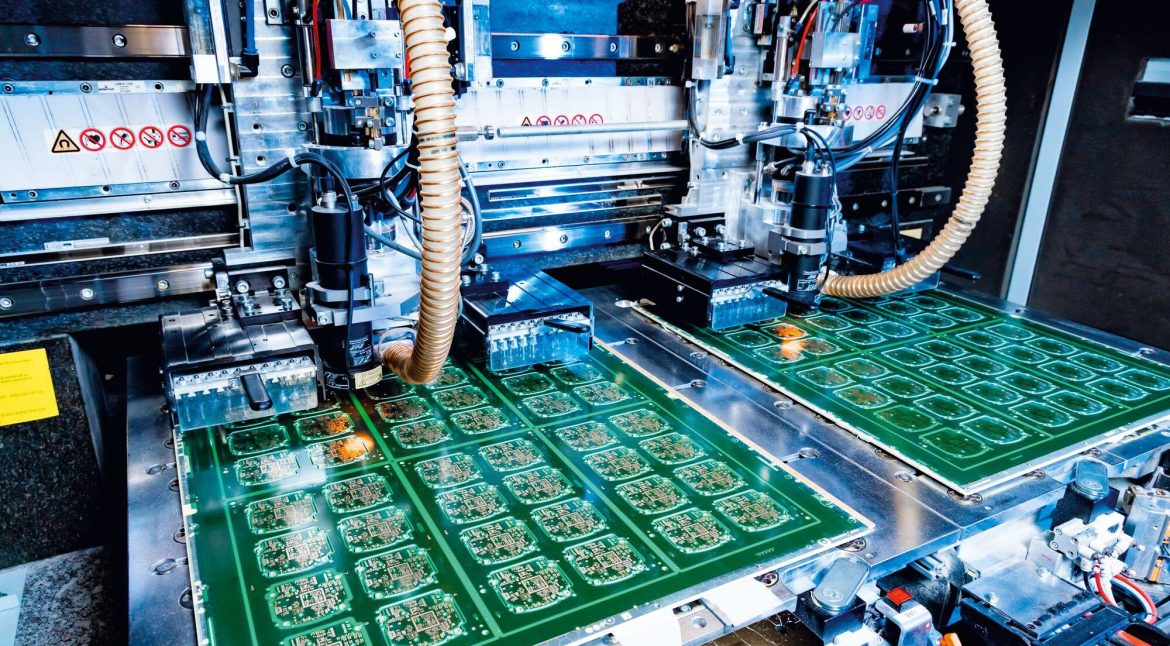
Automated pick-and-place equipment places surface-mount components onto the solder-pasted PCB.
For prototype projects, manufacturers may use a combination of automated and manual processes depending on:
- Production quantity
- Component package type
- Component availability
- Board complexity
- Required placement accuracy
- Prototype budget
Through-hole components are normally inserted manually or by dedicated insertion equipment.
Connectors, wires, terminals, jumpers, and mechanical components are then installed according to the assembly documentation.
Soldering
For SMT components, the assembled PCB normally passes through a reflow soldering process. The temperature profile must be carefully controlled to achieve reliable solder joints without damaging sensitive components.
PTH components can be soldered using selective soldering, wave soldering, or manual soldering depending on the design.
For prototypes, manual rework may occasionally be necessary. However, excessive manual intervention should be documented because it may affect the ability to reproduce the same results during mass production.
Inspection and Verification
Inspection is a critical part of prototype manufacturing.
Typical inspection methods include:
- Visual inspection
- Automated Optical Inspection (AOI)
- X-ray inspection
- Electrical testing
- In-Circuit Testing (ICT)
- Functional testing
The objective is not simply to determine whether the prototype works. Engineers also need to understand why it works or fails and whether the manufacturing process can reliably reproduce the result.
All important assembly and test results should be documented for future engineering revisions and production preparation.
Materials and Components Used in PCB Prototype Assembly


A prototype assembly uses essentially the same fundamental materials and electronic components found in production PCBs. However, prototype projects may use engineering samples, alternative components, or temporarily substituted parts when certain production components are unavailable.
PCB Substrate
The PCB substrate provides the mechanical structure and electrical insulation required by the circuit.
Common PCB materials include:
- FR-4
- High-Tg FR-4
- Polyimide
- PTFE-based materials
- Metal-core PCB materials
- Flexible PCB materials
The material should be selected according to electrical, thermal, mechanical, and environmental requirements.
Active Components
Active components require electrical power and can control, amplify, switch, or process electrical signals.
Common examples include:
- Diodes
- BJTs
- MOSFETs
- SCRs
- TRIACs
- Voltage regulators
- Operational amplifiers
- Microcontrollers
- Microprocessors
Different active devices perform different functions, such as switching, amplification, rectification, voltage regulation, and signal processing.
Passive Components
The most common passive components include:
- Resistors
- Capacitors
- Inductors
Resistors regulate current and establish voltage relationships. Capacitors store and release electrical energy and are widely used for filtering, decoupling, and energy storage. Inductors store energy in magnetic fields and are frequently used in power conversion and filtering circuits.
Integrated Circuits
Integrated circuits (ICs) integrate large numbers of electronic devices into a compact semiconductor package. Modern ICs can contain thousands, millions, or even billions of transistors depending on their function and process technology.
Examples include:
- Microcontrollers
- CPUs
- GPUs
- Memory devices
- Power management ICs
- Communication ICs
- RF devices
- Analog ICs
Selecting the correct IC package and footprint is particularly important during prototype development because package availability can influence both assembly feasibility and future production costs.
PCB Prototype Assembly Design Considerations
The main purpose of prototype assembly is to verify whether a design can ultimately become a reliable and manufacturable product. Therefore, engineers should consider manufacturing requirements from the earliest stages of PCB Design.
Component Availability
Whenever possible, designers should select standard components with established supply chains and multiple qualified sources.
Using difficult-to-source components during prototype development can result in:
- Extended lead times
- Higher component prices
- Prototype delays
- Component substitutions
- Additional qualification work
Engineers should also consider the long-term availability of components if the product is expected to enter mass production.
Design for Manufacturing (DFM)
DFM is essential for both prototype and production PCB development.
A design that works electrically may still be difficult or expensive to manufacture. DFM analysis helps identify issues such as:
- Insufficient component spacing
- Inadequate solder-mask clearance
- Improper pad dimensions
- Excessively narrow traces
- Difficult-to-access test points
- Component orientation problems
- Inappropriate hole sizes
- Insufficient copper spacing
A strong DFM process reduces rework and improves the transition from prototype to production.
Signal Integrity
Signal integrity becomes increasingly important as operating frequencies and data rates increase.
Engineers should carefully consider:
- Controlled impedance
- Differential-pair routing
- Trace length
- Return paths
- Ground-plane continuity
- Crosstalk
- Electromagnetic interference (EMI)
- Electromagnetic compatibility (EMC)
- Power integrity
High-speed interfaces such as USB, PCIe, DDR, Ethernet, and RF circuits require particularly careful PCB layout and stack-up design.
Thermal Management
Compact PCB layouts can generate significant localized heat. If thermal energy is not effectively dissipated, component temperatures may exceed recommended operating limits and reduce system reliability.
Common thermal-management techniques include:
- Thermal vias
- Copper heat-spreading areas
- Heatsinks
- Thermal pads
- Metal-core substrates
- Improved airflow
- Optimized component placement
Thermal imaging during prototype testing can help engineers identify unexpected hot spots and optimize the final design.
Testing Methods in PCB Prototype Assembly
Testing is one of the most important stages of PCB Prototype Assembly. A prototype should provide measurable evidence that the design performs as intended and can be manufactured consistently.
Visual Inspection
Visual inspection is the first level of quality control.
Engineers inspect the PCB for:
- Missing components
- Incorrect components
- Component misalignment
- Solder bridges
- Insufficient solder
- Excessive solder
- Damaged components
- PCB contamination
- Polarity errors
Visual inspection can be performed manually or supported by automated optical inspection equipment.
Automated Optical Inspection (AOI)
AOI systems use cameras and image-processing algorithms to inspect PCB assemblies for manufacturing defects.
AOI can detect problems such as:
- Missing components
- Incorrect component orientation
- Solder bridges
- Component displacement
- Soldering abnormalities
AOI is particularly valuable when the prototype process is intended to transition into automated mass production.
X-Ray Inspection
X-ray inspection is useful for components and solder joints that cannot be adequately inspected from the PCB surface.
It is commonly used for:
- BGA packages
- QFN packages
- Bottom-terminated components
- Hidden solder joints
- Internal voids
- Through-hole solder connections
In-Circuit Testing
ICT checks specific electrical characteristics of individual components and circuit nodes. Depending on the test strategy, it can identify incorrect component values, open circuits, short circuits, and other assembly-related defects.
For very small prototype quantities, however, the cost of developing a dedicated ICT fixture may not always be justified.
Functional Testing
Functional testing verifies whether the completed PCBA performs its intended function.
The board may be tested under actual operating conditions to evaluate:
- Input and output voltages
- Current consumption
- Communication interfaces
- Sensor performance
- Wireless connectivity
- Processor operation
- Power management
- Thermal behavior
- System-level functionality
Functional testing is particularly important because a PCB can pass visual inspection while still failing to meet system-level requirements.
Electrical Continuity Testing
Electrical testing can identify open circuits, short circuits, and unintended connections.
A multimeter can be useful for basic prototype verification, while automated electrical test systems are more appropriate for larger or more complex production volumes.
Benefits of PCB Prototype Assembly
Prototype assembly provides significant technical and commercial benefits before full-scale production begins.
Early Error Detection
Theoretical calculations and simulations cannot identify every real-world manufacturing or assembly problem.
Prototype assembly allows engineers to discover:
- PCB layout problems
- Incorrect footprints
- Component polarity issues
- Mechanical interference
- Soldering problems
- Thermal issues
- Signal integrity problems
- Unexpected power consumption
- Software-hardware interaction problems
Identifying these problems before mass production can prevent substantial financial losses.
Faster Design Modification
Prototype testing creates a practical feedback loop between design, manufacturing, and engineering teams.
When a problem is identified, engineers can modify the PCB layout, component selection, firmware, mechanical structure, or assembly process and build another prototype for verification.
This iterative approach is significantly less expensive than making major changes after production has started.
Better Production Readiness
A successful prototype provides valuable information for production planning.
Prototype results can help determine:
- Manufacturing parameters
- Component placement requirements
- Reflow profiles
- Inspection criteria
- Test procedures
- Assembly instructions
- Critical-to-quality (CTQ) characteristics
- Production tolerances
This information can then be transferred into the production documentation package.
Reduced Production Risk
Prototype assembly effectively acts as a risk-reduction stage between design and mass production.
The more complex the product, the more valuable this verification stage becomes. A well-tested prototype can significantly reduce the probability of expensive production failures.
Applications of PCB Prototype Assembly
PCB Prototype Assembly is widely used across electronics industries.
| Application | Typical Products | Key Benefits |
|---|---|---|
| Consumer Electronics | Smartphones, smart devices, home automation systems, PCs | Validates user experience, functionality, reliability, and product performance |
| Research & Development | Proof-of-concept devices, academic projects, technology demonstrations | Allows new technologies and concepts to be evaluated quickly |
| IoT | Smart sensors, monitoring systems, tracking devices, connected gateways | Verifies connectivity, power consumption, sensor performance, and peripheral compatibility |
| Industrial Electronics | Motor controllers, industrial sensors, automation equipment | Validates process parameters, electrical performance, and long-term reliability |
| Medical Electronics | Monitoring devices, diagnostic equipment, portable medical systems | Supports functional validation and reliability testing before commercialization |
| Automotive Electronics | Control modules, sensor systems, infotainment and ADAS electronics | Helps verify electrical, thermal, mechanical, and environmental performance |
Common Challenges in PCB Prototype Assembly
Although prototype assembly can reduce production risks, the process itself presents several challenges.
Design Errors
Errors in schematics, PCB layouts, BOMs, footprints, or assembly drawings can cause prototype failures.
A comprehensive engineering review should therefore be performed before fabrication. Designers should verify component orientation, polarity, footprints, net connections, mechanical clearances, and assembly documentation.
High-Density PCB Layouts
Modern products increasingly use fine-pitch BGAs, microcontrollers, high-speed interfaces, and compact RF modules.
High-density designs may require:
- Microvias
- HDI structures
- Fine-pitch components
- Controlled impedance
- Advanced PCB stack-ups
- Precision SMT placement
- X-ray inspection
These requirements increase manufacturing complexity and demand more advanced prototype capabilities.
Component Procurement
Prototype quantities are usually small, which can make component sourcing relatively expensive.
Common problems include:
- Minimum order quantities
- Long lead times
- Obsolete components
- Component shortages
- Engineering samples
- Authorized-source restrictions
Working with a manufacturer that has strong component sourcing capabilities can significantly reduce these risks.
Prototype Development Cost
The unit cost of a prototype is generally higher than the unit cost of mass production because fixed engineering, setup, programming, stencil, tooling, procurement, and testing costs are distributed across fewer boards.
However, the purpose of prototype manufacturing is not to achieve the lowest possible unit price. Its primary purpose is to validate the product and reduce the much greater financial risk associated with production-scale failures.
PCB Prototype Assembly vs. Mass Production
Prototype assembly and mass production serve different objectives.
| Feature | PCB Prototype Assembly | Mass Production |
|---|---|---|
| Primary objective | Design validation and engineering verification | High-volume commercial production |
| Production volume | Low | Medium to very high |
| Unit cost | Relatively high | Lower |
| Design flexibility | Very high | Relatively limited |
| Engineering changes | Easy to implement | More expensive and time-consuming |
| Setup cost | Distributed across a small quantity | Distributed across a large quantity |
| Testing | Comprehensive engineering validation | Optimized production testing |
| Manufacturing focus | Flexibility and learning | Efficiency, consistency, and throughput |
A common development strategy is therefore:
Concept → PCB Design → Prototype → Testing → Design Revision → Pilot Production → Mass Production
This staged approach allows manufacturers to progressively reduce technical and commercial risks.
How to Choose a PCB Prototype Assembly Partner
Choosing the right manufacturing partner is essential for obtaining meaningful prototype results. The ideal supplier should not simply assemble the PCB but should also provide engineering support throughout the development process.
Technical Capability
Evaluate whether the manufacturer can handle the technologies required by your design, including:
- Fine-pitch SMT
- BGA and QFN assembly
- PTH assembly
- Mixed-technology assembly
- HDI PCB fabrication
- Flexible and rigid-flex PCBs
- High-speed PCB designs
- RF PCB assembly
Quality Control and Testing
A capable supplier should have appropriate inspection and testing equipment, such as:
- AOI
- X-ray inspection
- Electrical testing
- Functional testing
- Microscopic inspection
- Thermal testing when required
The supplier should also maintain traceable production and inspection records.
DFM Engineering Support
A strong prototype partner should review your PCB files before production and identify manufacturing risks.
The DFM review should cover:
- PCB fabrication rules
- Component footprints
- Assembly clearances
- Solder-mask requirements
- Component availability
- PCB stack-up
- Testing access
- Thermal considerations
Component Sourcing Capability
A reliable component supply chain can substantially reduce prototype lead times. The manufacturer should be able to source components from reputable and traceable suppliers and provide alternatives when original parts are unavailable.
Prototype-to-Production Capability
Ideally, the same manufacturing partner should be capable of supporting the project from prototype through pilot production and mass production.
This reduces the need to transfer technical data between multiple suppliers and helps maintain consistency between prototype and production versions.
Conclusion
PCB Prototype Assembly is a critical stage in modern electronics product development. It transforms a theoretical PCB Design into a physical, testable product and provides engineers with valuable information about electrical performance, manufacturability, thermal behavior, component selection, and system reliability.
By using prototype assembly before mass production, manufacturers can identify design errors early, optimize component selection, validate assembly processes, improve PCBA reliability, and reduce the financial risks associated with large-scale production.
As electronic products continue to become smaller, faster, and more intelligent, prototype manufacturing is also becoming more sophisticated. Automation, AI-assisted design analysis, advanced simulation, high-precision SMT placement, automated inspection, 3D modeling, and rapid manufacturing technologies are helping engineers shorten development cycles and improve prototype quality.
For companies developing new electronic products, selecting an experienced PCB manufacturing and assembly partner can make a significant difference. Kingda can support PCB development from design review and prototype fabrication to component assembly, inspection, testing, and production preparation, helping customers move from engineering concepts to reliable production-ready electronic products.