In today’s competitive electronics industry, bringing a new product to market quickly while maintaining reliable performance is a major challenge for OEMs, product developers, and engineering teams.
Before committing to mass production, most companies build and test a PCB prototype to verify the circuit design, identify potential problems, evaluate component placement, and confirm that the product can be manufactured successfully.
PCB prototype manufacturing provides an important bridge between electronic design and production. Instead of discovering design or manufacturing problems after thousands of boards have been produced, engineers can identify and correct issues during the prototype stage.
For electronics companies, a well-managed prototype PCB assembly process can reduce development risk, control costs, improve product reliability, and accelerate the transition from engineering validation to production.
As an experienced PCB manufacturer and PCB assembly service provider, Kingda provides PCB prototype manufacturing, rapid PCB prototyping, prototype PCB assembly, component sourcing, SMT, THT, testing, and engineering support to help customers move from initial design concepts to reliable production.
What Is a PCB Prototype?
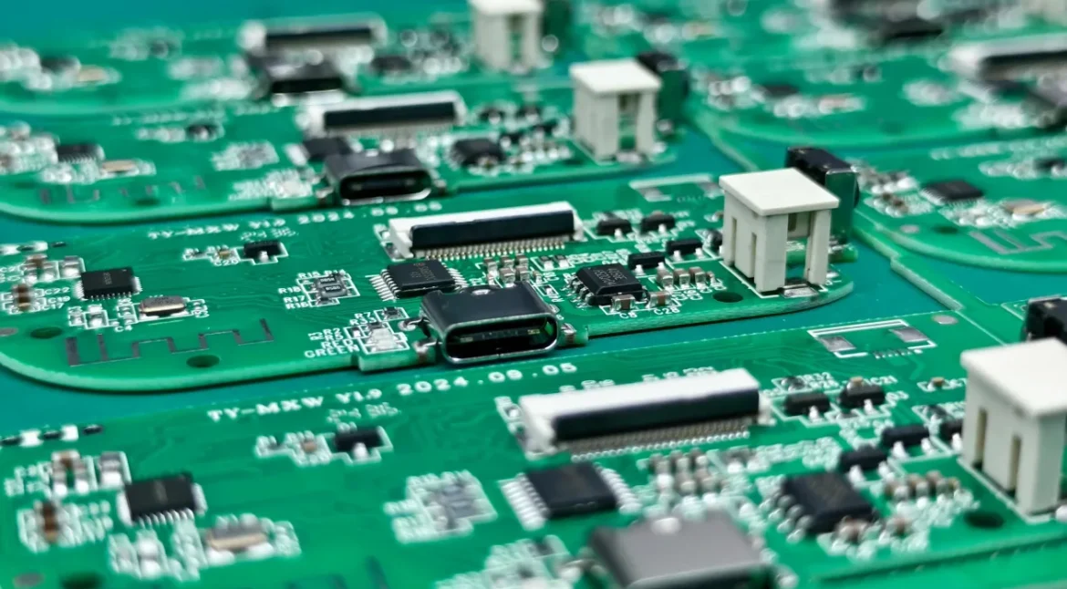
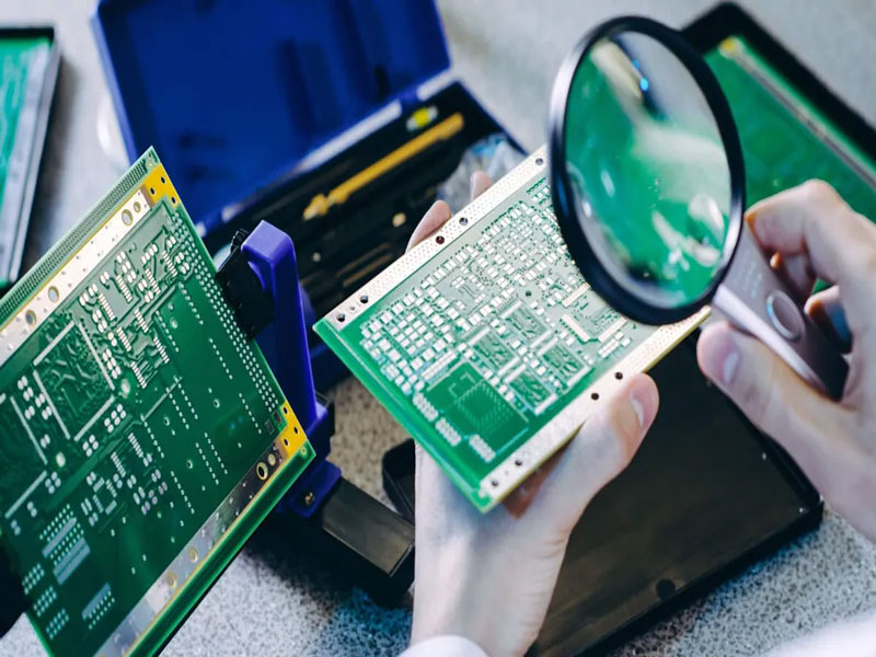
A PCB prototype is an early production version of a printed circuit board used to verify an electronic design before full-scale manufacturing.
A PCB prototype is not necessarily a smaller version of the final PCB. Instead, it is a limited production build manufactured according to the intended design so engineers can evaluate the board’s electrical, mechanical, thermal, and manufacturing performance.
Depending on the product, a prototype PCB may be used to verify:
- Circuit functionality
- PCB layout
- Component placement
- Signal integrity
- Power distribution
- Thermal performance
- Mechanical dimensions
- Connector locations
- Firmware operation
- Manufacturing feasibility
- Assembly processes
The objective is simple:
Find problems early, when they are easier and less expensive to correct.
PCB Prototype Manufacturing vs. PCB Prototype Assembly
PCB prototyping normally involves two related but different stages.
1. PCB Prototype Manufacturing
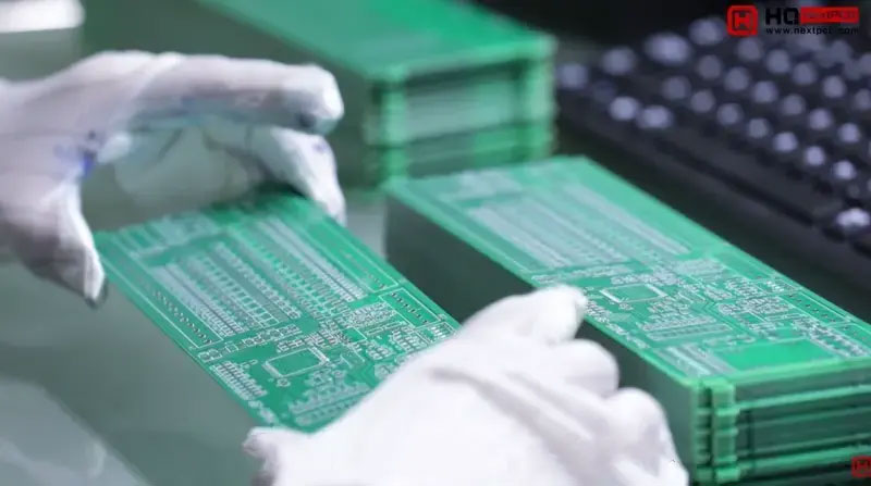
The first stage is the fabrication of the bare PCB.
The manufacturer converts the customer’s PCB design data into a physical circuit board.
Depending on the project, this may involve:
- Single-layer PCB
- Double-sided PCB
- Multilayer PCB
- HDI PCB
- High-frequency PCB
- High-speed PCB
- Flexible PCB
- Rigid-flex PCB
The fabrication process may include:
- PCB imaging
- Etching
- Drilling
- Plating
- Lamination
- Solder mask
- Surface finishing
- Electrical testing
- Final inspection
At this stage, engineers can evaluate whether the PCB stack-up, materials, routing, dimensions, and manufacturing structure are suitable for the intended application.
2. Prototype PCB Assembly
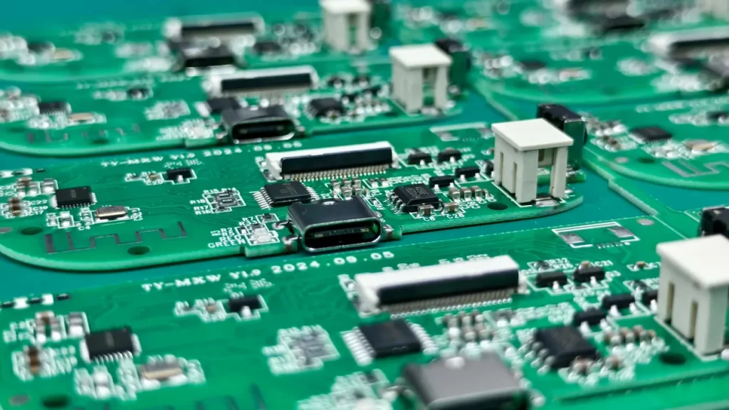
After the bare PCB is manufactured, electronic components are installed to create a functional PCBA.
A prototype PCB assembly may include:
- SMT assembly
- Through-hole assembly
- Component placement
- Solder paste printing
- Reflow soldering
- Selective soldering
- Manual assembly
- Programming
- Electrical testing
- Functional testing
The assembled prototype allows engineers to evaluate the actual behavior of the electronic product rather than simply inspecting the PCB layout.
Why Is PCB Prototyping Important?
1. Identify Design Problems Early
One of the biggest advantages of PCB prototyping is early detection of design problems.
A prototype may reveal:
- Incorrect component placement
- PCB layout conflicts
- Signal integrity problems
- Power distribution issues
- Thermal problems
- Incorrect connector positioning
- Insufficient clearance
- Manufacturing limitations
Fixing these problems during prototype development is normally much less expensive than correcting them after mass production begins.
For example, changing a PCB layout before production may only require an engineering revision. Discovering the same problem after several thousand boards have been manufactured can result in PCB scrap, component waste, rework, and schedule delays.
2. Reduce Production Risk
Moving directly from a CAD design to mass production creates unnecessary manufacturing risk.
A PCB prototype allows engineers to validate:
- PCB fabrication
- Component availability
- Assembly processes
- Soldering performance
- Programming
- Electrical performance
- Functional testing
- Mechanical integration
The prototype therefore acts as a manufacturing checkpoint before larger production quantities are released.
For OEMs and product developers, this can significantly reduce the risk of expensive production problems.
3. Verify Component Placement
A PCB design may look correct on a computer screen but behave differently when it becomes a physical assembly.
Prototype testing allows engineers to verify:
- Component positioning
- Connector accessibility
- Cable routing
- Component clearance
- Heat-generating component locations
- Mechanical mounting
- Enclosure integration
- Serviceability
This is particularly important for compact electronic products where available PCB space is limited.
4. Evaluate Electrical and Thermal Performance
A prototype PCB can provide valuable information about actual operating conditions.
Engineers can measure:
- Voltage
- Current
- Power consumption
- Temperature
- Signal quality
- Communication performance
- Electromagnetic behavior
- Thermal distribution
The test results can then be used to improve the next PCB revision.
This iterative process is one of the fundamental advantages of rapid PCB prototype manufacturing.
5. Validate Manufacturing Feasibility
A design may be electrically functional but difficult to manufacture.
Prototype production can reveal:
- Difficult component spacing
- Fine-pitch assembly challenges
- BGA routing limitations
- Excessive solder paste
- QFN soldering issues
- PCB warpage
- Difficult inspection areas
- Insufficient test points
A professional PCB prototype manufacturer can provide DFM and DFA feedback before production, helping engineering teams identify manufacturing risks early.
6. Accelerate Product Development
Speed is critical during new product development.
A reliable rapid PCB prototype service can shorten the time between:
Design → PCB Fabrication → Assembly → Testing → Engineering Revision
Instead of waiting for a large production cycle, engineering teams can quickly build physical boards, test them, identify problems, and implement the next design revision.
This creates a faster development loop and can help companies reach the market sooner.
PCB Prototype Manufacturing Process
A professional PCB prototype manufacturing process normally includes several stages.
Step 1: Engineering Data Review
The manufacturer reviews the customer’s:
- Gerber files
- ODB++ files
- IPC-2581 files
- BOM
- Pick-and-place files
- Assembly drawings
- Stack-up information
- Impedance requirements
- Special manufacturing instructions
The objective is to identify missing or inconsistent information before production.
Step 2: DFM and DFA Review
Design for Manufacturing (DFM) evaluates whether the PCB can be fabricated reliably.
Typical considerations include:
- Trace and spacing
- Drill size
- Annular ring
- Solder mask
- Via structure
- Stack-up
- Copper distribution
- Impedance requirements
- Panelization
Design for Assembly (DFA) focuses on the assembly process.
It may evaluate:
- Component spacing
- Component orientation
- Pin 1 marking
- Fiducials
- BGA placement
- QFN pads
- Stencil design
- Test points
- Through-hole accessibility
Step 3: PCB Fabrication
The PCB is manufactured according to the approved engineering data.
Depending on the application, the board may use:
- FR-4
- High-Tg materials
- High-frequency materials
- Flexible materials
- Metal-core materials
- HDI structures
Surface finishes may include:
- ENIG
- HASL
- Lead-free HASL
- OSP
- Immersion silver
The appropriate material and surface finish should be selected according to electrical, thermal, mechanical, and assembly requirements.
Step 4: Component Sourcing
Components can be supplied by the customer or sourced by the manufacturer.
A complete prototype PCB assembly service may support:
- Customer-supplied components
- Partial turnkey sourcing
- Full turnkey component sourcing
Component sourcing is particularly important for prototypes because small quantities of specialized components may be difficult or expensive to obtain.
Step 5: SMT and THT Assembly
After the bare PCB and components are ready, the assembly process begins.
Typical SMT processes include:
- Solder paste printing
- SPI
- Pick and place
- Reflow soldering
- AOI
- X-ray inspection where required
Through-hole components can then be installed using:
- Manual soldering
- Wave soldering
- Selective soldering
The appropriate process depends on the component mix and product requirements.
Step 6: Electrical and Functional Testing
The assembled prototype should be tested according to the engineering requirements.
Possible testing methods include:
- Visual inspection
- Flying probe
- ICT
- Electrical testing
- Programming verification
- Functional testing
Functional testing is particularly important because it verifies whether the completed PCBA actually performs its intended function.
PCB Prototype vs. Low Volume PCB Assembly
A prototype and a low-volume production build are related, but they have different objectives.
| Factor | PCB Prototype | Low Volume Production |
|---|---|---|
| Main objective | Validate design | Validate repeatable production |
| Quantity | Usually very small | Small production batch |
| Design changes | Frequent | Controlled |
| Testing | Engineering validation | Production testing |
| Documentation | Development-focused | Manufacturing-controlled |
| Yield | Learning objective | Important production KPI |
| Traceability | May be limited | More comprehensive |
| Process repeatability | Secondary | Critical |
A useful development path is:
PCB Design → PCB Prototype → Prototype PCB Assembly → Design Validation → Low Volume Production → Mass Production
This staged approach helps reduce technical and manufacturing risk.
How Many PCB Prototypes Should You Build?
There is no universal number of prototype boards.
The appropriate quantity depends on the complexity of the design and the purpose of the build.
Typical quantities may include:
| Development Stage | Typical Quantity |
|---|---|
| Initial engineering prototype | 1–5 |
| Design validation | 5–20 |
| Functional validation | 10–50 |
| Pilot production | 20–200+ |
For early engineering work, a very small quantity may be sufficient.
For more complex projects, additional prototypes may be useful for:
- Electrical testing
- Mechanical testing
- Environmental testing
- Reliability testing
- Firmware development
- Customer evaluation
- Compliance testing
The objective is not to maximize prototype quantity, but to obtain enough physical data to make a confident production decision.
Rapid PCB Prototype Manufacturing
Speed is an important factor in product development.
A rapid PCB prototype manufacturer should be able to coordinate:
- Engineering review
- PCB fabrication
- Component sourcing
- SMT assembly
- Testing
- Shipping
Reducing the number of separate suppliers can shorten the overall development cycle.
Kingda provides integrated PCB manufacturing and assembly services, allowing customers to manage PCB fabrication, component procurement, assembly, and testing through one manufacturing partner.
For projects where materials and production requirements are ready, Kingda supports rapid-response prototype and PCB assembly services, with delivery schedules depending on PCB complexity, component availability, assembly requirements, and testing requirements.
Quality Control for PCB Prototypes
Prototype production should not be treated as uncontrolled experimental work.
Even when only a few boards are manufactured, appropriate quality controls remain important.
A professional PCB prototype manufacturer may use:
- Incoming inspection
- SPI
- AOI
- X-ray
- Electrical testing
- Functional testing
- Final inspection
SPI
Solder Paste Inspection (SPI) evaluates solder paste deposition before component placement and reflow.
It can identify:
- Insufficient paste
- Excessive paste
- Offset
- Printing variation
AOI
Automated Optical Inspection (AOI) can identify:
- Missing components
- Incorrect components
- Reversed components
- Component displacement
- Visible solder defects
X-Ray
X-ray inspection provides visibility into hidden solder joints.
It is particularly useful for:
- BGA
- QFN
- LGA
- Bottom-terminated components
Functional Testing
Functional testing verifies whether the assembled prototype performs according to the intended product specifications.
Depending on the product, this may include:
- Power-up testing
- Communication testing
- Sensor testing
- Display testing
- Motor control
- Network communication
- System-level operation
Documentation and Revision Control
Revision control is particularly important during PCB prototype development because engineering changes may happen frequently.
A controlled prototype package should identify:
- PCB revision
- BOM revision
- Assembly drawing revision
- Firmware version
- Test software version
- Approved deviations
- Component substitutions
A common development problem occurs when the PCB is updated but the BOM or pick-and-place file remains unchanged.
A professional manufacturing partner should help identify these inconsistencies before production.
Common PCB Prototype Design Problems
Insufficient Component Clearance
Components that are too close together may create:
- Assembly difficulties
- Inspection problems
- Rework challenges
Incorrect Component Orientation
Incorrect polarity or pin-1 orientation can cause immediate functional failures.
Poor Test-Point Planning
Without sufficient test points, electrical testing and debugging may become more difficult.
Inadequate Thermal Design
High-power components may require:
- Larger copper areas
- Thermal vias
- Heatsinks
- Better component placement
- Improved airflow
Difficult BGA Routing
Fine-pitch BGA devices may require:
- HDI PCB
- Laser microvias
- Via-in-pad
- Additional routing layers
PCB technology should be selected based on the actual package, routing density, board size, and electrical requirements.
How to Choose a PCB Prototype Manufacturer
Choosing the right PCB prototype manufacturer can have a significant effect on development speed and product quality.
1. PCB Manufacturing Capability
Check whether the supplier can support the required:
- Layer count
- PCB thickness
- Copper weight
- Trace and spacing
- Via technology
- HDI
- High-frequency materials
- Controlled impedance
2. Prototype PCB Assembly Capability
The supplier should be able to handle:
- SMT
- THT
- BGA
- QFN
- LGA
- Fine-pitch components
- Double-sided assembly
- Selective soldering
3. Component Procurement
A supplier with component sourcing capability can reduce procurement complexity and help manage:
- Lead times
- Part availability
- Approved substitutions
- Small-quantity purchasing
4. Engineering Support
Look for a supplier that provides:
- DFM
- DFA
- BOM review
- PCB design feedback
- Manufacturing optimization
- Process recommendations
5. Inspection and Testing
A professional supplier should offer appropriate inspection and testing capabilities, including:
- SPI
- AOI
- X-ray
- Electrical testing
- ICT
- Functional testing
6. Ability to Scale
The ideal supplier should support the complete development path:
Prototype → Validation → Low Volume → Production
This avoids the need to transfer the project to a completely different manufacturer after prototype validation.
Why Choose Kingda for PCB Prototype Manufacturing?
Kingda provides integrated PCB prototype manufacturing and prototype PCB assembly services for electronics companies, OEMs, product developers, and engineering teams.
Instead of separating PCB fabrication, component sourcing, assembly, and testing among multiple suppliers, customers can work with Kingda through an integrated manufacturing workflow.
One-Stop PCB and PCBA Services
Kingda provides services covering:
- PCB manufacturing
- PCB prototype manufacturing
- Prototype PCB assembly
- SMT assembly
- THT assembly
- Component sourcing
- PCB testing
- Functional testing
- Final assembly
This integrated model can simplify communication and reduce the coordination required between different suppliers.
Flexible Prototype Quantities
Prototype requirements vary significantly between projects.
Kingda supports flexible PCB and PCBA production quantities, including prototype orders and small-volume builds.
This allows customers to validate designs without immediately committing to large production quantities.
DFM and Engineering Support
Kingda’s engineering support can help customers review their designs before manufacturing.
Engineering services may include:
- PCB design review
- DFM analysis
- DFA analysis
- BOM review
- Manufacturing optimization
- Process improvement
The objective is to identify potential problems before they become production problems.
Advanced PCB Manufacturing
Kingda supports a broad range of PCB technologies, including:
- Multilayer PCB
- HDI PCB
- High-frequency PCB
- High-speed PCB
- Flexible PCB
- Rigid-flex PCB
- Blind and buried vias
This allows prototype projects to use the same underlying PCB technology that may later be required for production.
Complete PCB Assembly
Kingda’s prototype PCB assembly capabilities cover both SMT and through-hole technologies.
Depending on project requirements, production may include:
- Fine-pitch SMT
- BGA
- QFN
- Small passive components
- Double-sided SMT
- Through-hole assembly
- Selective soldering
- Programming
- Testing
Inspection and Testing
Kingda supports manufacturing inspection and testing technologies including:
- SPI
- AOI
- X-ray
- ICT
- Electrical testing
- Functional testing
This allows customers to select an appropriate quality-control strategy based on product complexity.
From Prototype to Mass Production
One of the major advantages of working with an integrated PCB manufacturer is scalability.
The same manufacturing partner can support:
PCB Prototype → Prototype Assembly → Design Validation → Low Volume Production → Mass Production
This continuity can reduce the risks associated with transferring a validated design to a new manufacturing supplier.
Conclusion
PCB prototype manufacturing is an essential stage in modern electronic product development.
A well-designed and properly assembled prototype allows engineering teams to identify design problems, validate components, evaluate electrical and thermal performance, verify mechanical integration, and assess manufacturing feasibility before committing to larger production quantities.
A professional prototype PCB assembly process should include more than PCB fabrication and component placement. It should combine DFM/DFA engineering, component sourcing, SMT, THT, inspection, electrical testing, functional testing, documentation, and revision control.
For OEMs, electronics developers, and manufacturers, the ideal PCB partner should be capable of supporting the entire product lifecycle.
Kingda provides integrated PCB prototype manufacturing, PCB assembly, component sourcing, engineering support, testing, and production services, helping customers move efficiently from initial design validation to low-volume and mass production.
With the right manufacturing partner, PCB prototyping becomes more than a test stage. It becomes a controlled path toward a reliable, manufacturable, and production-ready electronic product.