What Is a PCB Prototype?
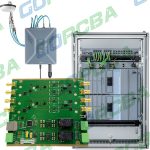
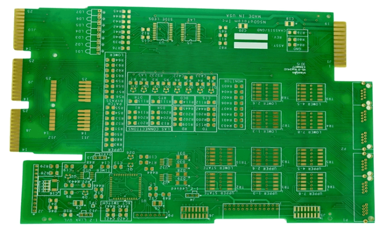
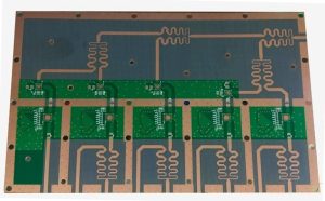
A PCB Prototype is an initial physical version of a printed circuit board manufactured to verify whether the design meets its electrical, mechanical, thermal, and functional requirements before entering full-scale production.
Unlike a finished production PCB, a prototype is primarily used for design validation and engineering verification. Engineers can manufacture a small quantity of prototype boards, assemble components, perform functional and reliability tests, identify potential problems, and modify the design based on test results.
The prototyping process may involve several design iterations. Changes can be made to the schematic, PCB layout, component selection, materials, stackup, routing, or manufacturing process before the design is released for mass production.
A typical PCB Prototype project follows a development cycle such as:
Design → Prototype Manufacturing → PCB Assembly → Testing → Evaluation → Design Optimization → Final Production
This iterative approach allows manufacturers and design teams to identify problems earlier and reduce the technical and financial risks associated with launching a new electronic product.
For complex products, prototype production can also be combined with a small pre-production run. This provides additional information about manufacturing consistency, assembly performance, testing requirements, and production scalability.
Benefits of PCB Prototyping Services
Early Detection of Design Problems
One of the most important advantages of PCB Prototyping is the ability to identify potential problems before mass production.
During prototype development, design engineers, manufacturing engineers, test engineers, and product teams can evaluate the physical board and compare actual performance with the original design requirements.
Testing may reveal issues such as:
- Incorrect component footprints
- Routing conflicts
- Signal integrity problems
- Power distribution issues
- Excessive temperature rise
- Electromagnetic interference
- Mechanical interference
- Soldering or assembly problems
- Insufficient test points
- Manufacturing tolerance issues
Simulation and design analysis can identify many potential problems, but physical prototypes provide valuable real-world information that cannot always be obtained from simulation alone.
Reduced Product Development Risk
A prototype allows engineers to verify the design before committing to a large production quantity.
If a problem is discovered during prototype testing, only a limited number of boards need to be modified or remanufactured. Correcting the same problem after mass production begins can result in significantly higher costs due to material waste, production downtime, rework, field failures, or customer returns.
Therefore, PCB Prototype Manufacturing acts as an important risk-control stage between PCB design and volume production.
Design Optimization
The first PCB design is not always the final or optimal solution.
Prototype testing may reveal opportunities to improve component placement, routing, thermal management, circuit performance, assembly efficiency, or overall board dimensions.
Engineers can use prototype results to optimize:
- PCB layout
- Component selection
- Copper distribution
- Trace width and spacing
- Power and ground structures
- Thermal management
- Signal routing
- Mechanical dimensions
- Manufacturing processes
This iterative approach can improve product performance while reducing unnecessary production costs.
More Accurate Requirement Definition
Building a physical prototype can also reveal requirements that may not have been fully defined at the beginning of a project.
For example, actual prototype testing may show that additional test points are required, a connector needs to be repositioned, a component generates more heat than expected, or a particular assembly process requires additional clearance.
These findings allow engineers and customers to refine technical specifications before production begins.
Better Reliability Verification
Reliability testing is an important part of prototype development for products that operate under demanding environmental conditions.
Depending on the application, prototype boards may be evaluated under temperature cycling, humidity, vibration, mechanical stress, electrical load, or other environmental conditions.
The purpose is to determine whether the PCB and assembled components can maintain their required performance throughout the expected operating conditions.
Key Factors in PCB Prototype Services
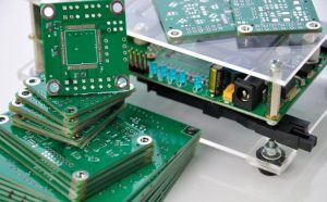
The quality of a prototype depends not only on the PCB fabrication process but also on engineering support, material selection, testing capabilities, component sourcing, and production management.
Short Lead Time
Speed is one of the most important requirements for Rapid PCB Prototype services.
A shorter prototype cycle allows engineers to complete testing sooner and move through design iterations more quickly.
However, rapid delivery should not come at the expense of manufacturing quality. An effective prototype manufacturer should balance production speed with engineering review, process control, inspection, and testing.
The actual lead time depends on factors such as:
- Number of PCB layers
- Board dimensions
- Material availability
- Line width and spacing
- Via technology
- Surface finish
- Component availability
- PCB Assembly requirements
- Testing requirements
One-Stop Prototype Services
A one-stop PCB Prototype Services provider can support multiple stages of the product development process.
Depending on project requirements, services may include:
Engineering Review → PCB Fabrication → Component Sourcing → PCB Assembly → Inspection → Electrical Testing → Functional Testing
Using an integrated workflow can reduce communication gaps between different suppliers and make it easier to manage design changes.
For customers developing new products, having PCB fabrication and assembly coordinated by one experienced manufacturer can also simplify project management and shorten the overall development cycle.
High Manufacturing Quality
Prototype boards must accurately represent the intended production design.
Poor-quality prototypes can produce misleading test results. For example, unexpected electrical performance could result from fabrication defects rather than the actual circuit design.
Therefore, prototype manufacturing should maintain appropriate control over:
- Layer registration
- Copper thickness
- Trace width and spacing
- Hole size and position
- Via quality
- Board thickness
- Surface finish
- Solder mask
- Impedance
- Electrical connectivity
High-quality prototype manufacturing provides a more reliable foundation for engineering validation.
Advanced PCB Technologies
Modern PCB Prototype Manufacturing is not limited to simple single- or double-sided boards.
Depending on the manufacturer’s capabilities, prototype services can support advanced technologies such as:
- Multilayer PCB
- HDI PCB
- Flexible PCB
- Rigid-Flex PCB
- High-frequency PCB
- High-Tg PCB
- Heavy-copper PCB
- Blind and buried vias
- Microvias
- Controlled-impedance PCB
- Metal-core PCB
Prototype capability is particularly important when developing high-speed, high-density, RF, automotive, medical, aerospace, or other specialized electronic products.
Flexible Quantities
Prototype projects typically require smaller quantities than mass production.
A manufacturer should therefore be able to support low-volume prototype orders while maintaining consistent quality.
After prototype verification, the same project can then transition to pilot production and eventually volume manufacturing.
This provides a smoother path from initial concept to commercial production.
Competitive Cost
The purpose of prototyping is not simply to produce the cheapest possible PCB. The objective is to obtain useful engineering information while controlling development costs.
An effective PCB Prototyping strategy can reduce total project costs by identifying design problems before expensive mass production begins.
A slightly higher prototype cost can therefore be justified if it provides better testing coverage, faster engineering feedback, or more reliable production validation.
What Are the Steps for Making a PCB Prototype?
The exact process varies according to the PCB structure and project requirements, but a typical PCB Prototype workflow includes the following steps.
1. Schematic Capture
The development process begins with an electronic schematic created using an Electronic Design Automation (EDA) tool.
The schematic defines the electrical relationships between components and establishes the functional architecture of the circuit.
Engineers verify component values, electrical connections, power requirements, interfaces, and other fundamental design parameters before moving to PCB layout.
At this stage, Design for Manufacturing (DFM) should also be considered.
DFM analysis helps identify potential manufacturing problems before fabrication, including insufficient spacing, unsuitable hole sizes, difficult-to-manufacture geometries, and other design-rule violations.
2. PCB Prototype Layout
The schematic is then converted into a physical PCB layout.
During layout, engineers determine the position of components, routing paths, copper areas, power and ground structures, vias, mounting holes, connectors, and test points.
For high-speed circuits, designers must also consider:
- Controlled impedance
- Signal return paths
- Differential-pair routing
- Crosstalk
- Power integrity
- Electromagnetic compatibility
- Via transitions
- Reference planes
A Design Rule Check (DRC) is normally performed before the design is released for manufacturing.
3. Engineering Review and DFM Analysis
Before fabrication, the PCB design files are reviewed by the manufacturing engineering team.
The review may include:
- Layer count
- Board thickness
- Material selection
- Copper thickness
- Minimum line width and spacing
- Drill sizes
- Annular rings
- Via structures
- Solder mask clearances
- Surface finish
- Impedance requirements
- Panelization
- Manufacturing tolerances
The goal is to ensure that the design can be manufactured reliably using the available production processes.
4. PCB Fabrication
Once the design is approved, the physical prototype board is manufactured.
The manufacturing process depends on the PCB structure but may include:
Material Preparation → Inner-Layer Imaging → Etching → AOI → Lamination → Drilling → Copper Plating → Outer-Layer Imaging → Solder Mask → Surface Finish → Electrical Testing → Routing
Gerber, ODB++, drill, stackup, and other manufacturing data provide the information required to fabricate the board.
5. Component Sourcing
If the project requires assembled prototypes, components must be sourced according to the approved bill of materials (BOM).
Component availability can significantly affect prototype lead time.
Engineers should verify:
- Manufacturer part number
- Package type
- Component value
- Lifecycle status
- Alternative components
- Quantity requirements
- Special procurement requirements
Using the correct components is essential because prototype test results depend on the actual components installed on the board.
6. PCB Assembly
The fabricated PCB is assembled using the required assembly process.
Depending on the design, this may include SMT placement, through-hole assembly, reflow soldering, selective soldering, or manual assembly.
During prototype assembly, particular attention should be paid to component orientation, polarity, solder-joint quality, fine-pitch packages, and thermal-sensitive components.
7. PCB Prototype Testing
Testing is a critical stage of PCB Testing.
Electrical testing can verify circuit continuity and identify potential opens or shorts. Flying-probe testing is commonly used for low-volume prototypes because it does not require a dedicated test fixture.
Functional testing can then evaluate whether the assembled board performs according to its intended specifications.
Depending on the product, testing may include:
- Electrical continuity testing
- Insulation testing
- Functional testing
- Power-up testing
- Signal integrity testing
- Thermal testing
- Communication interface testing
- Environmental testing
- Reliability testing
The test plan should be established before prototype production whenever possible.
8. Design Evaluation and Iteration
After testing, engineers analyze the prototype results and compare them with the original specifications.
If problems are discovered, the design can be revised and another prototype produced.
Common modifications include changing component values, adjusting trace routing, adding test points, changing component placement, modifying the PCB stackup, improving thermal management, or changing the mechanical structure.
This iterative process continues until the design meets the required performance and reliability targets.
PCB Prototype Testing Considerations
Testing should be planned as early as possible because the PCB design can directly affect how easily the finished prototype can be tested.
Test Points
Adequate test points allow engineers to access important electrical nodes during testing.
If test points are not considered during PCB layout, engineers may have difficulty connecting probes or automated test equipment to critical signals.
Connectors and Sockets
Connectors, sockets, and test interfaces should be selected according to the intended testing method.
Mechanical clearance, accessibility, electrical characteristics, and repeated connection requirements should all be considered.
Test Equipment
Different prototype designs require different test equipment.
Simple boards may only require electrical continuity testing and basic laboratory instruments, while advanced products may require oscilloscopes, logic analyzers, network analyzers, thermal cameras, environmental chambers, or specialized functional test systems.
Reliability Testing
For products expected to operate under harsh conditions, prototype reliability testing may include:
- Temperature cycling
- High-temperature operation
- Low-temperature operation
- Humidity exposure
- Vibration testing
- Mechanical shock
- Electrical load testing
The exact test conditions should be based on the product’s intended operating environment and applicable industry standards.
PCB Prototype vs. Mass Production
PCB prototypes and production PCBs serve different purposes.
| Feature | PCB Prototype | Mass Production PCB |
|---|---|---|
| Primary purpose | Design verification | Commercial production |
| Typical quantity | Low | Medium to high |
| Main focus | Testing and optimization | Consistency and efficiency |
| Design changes | Relatively frequent | Usually controlled |
| Production setup | Flexible | Highly optimized |
| Cost per board | Higher | Lower |
| Manufacturing priority | Speed and validation | Efficiency and repeatability |
A successful prototype does not automatically guarantee successful mass production.
Before volume production, manufacturers should also verify process capability, material availability, assembly yield, testing methods, quality controls, and production scalability.
Why Choose Kingda for PCB Prototype Services?
Selecting the right PCB Prototype Services provider can significantly influence the efficiency of product development.
Kingda can support customers throughout the transition from PCB design to prototype manufacturing, assembly, testing, and production preparation.
Our engineering-focused approach helps customers identify potential design and manufacturing risks at an early stage.
Fast Prototype Turnaround
Kingda supports rapid prototype manufacturing to help customers shorten development cycles and complete engineering verification sooner.
Production schedules can be coordinated according to board complexity, materials, quantity, assembly requirements, and testing needs.
Competitive Pricing
Prototype development should provide reliable engineering results while maintaining reasonable development costs.
Kingda can provide flexible manufacturing solutions based on prototype quantity, PCB structure, materials, assembly requirements, and testing specifications.
Reliable Prototype Quality
Prototype boards are manufactured according to the customer’s design data and applicable quality requirements.
Process control and inspection are applied throughout PCB fabrication to help ensure that prototype results accurately reflect the intended design.
Engineering and Manufacturing Expertise
An experienced engineering team can provide feedback when a design presents potential manufacturing risks.
Kingda can review factors such as PCB stackup, trace geometry, drill requirements, materials, component placement, thermal considerations, and assembly requirements.
Early engineering communication can help reduce unnecessary redesigns and improve the transition from prototype to production.
Support from Prototype to Production
The ultimate purpose of prototyping is to prepare a reliable design for commercial manufacturing.
Kingda can support projects through different development stages, helping customers move from:
PCB Design → Prototype → PCB Assembly → Testing → Design Optimization → Pilot Production → Mass Production
This integrated approach can reduce communication gaps and make the transition to volume production more efficient.
Conclusion
A PCB Prototype is an essential step in modern electronic product development. It provides engineers with a physical platform for validating electrical performance, mechanical design, thermal behavior, assembly processes, and overall product functionality.
Through PCB Prototyping, potential design and manufacturing problems can be discovered before large-scale production, reducing development risk and unnecessary costs.
A successful prototype program should combine accurate PCB fabrication, reliable component sourcing, professional PCB Assembly, comprehensive PCB Testing, and effective engineering feedback.
For complex products, selecting an experienced manufacturing partner such as Kingda can help streamline the entire development process and provide a smoother transition from the first prototype to stable mass production.