PCB Reverse Engineering Cost: Complete 2026 Guide
What PCB Reverse Engineering Covers
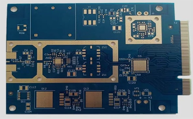
Reverse engineering a printed circuit board means reconstructing the design data from a physical sample. The end product is usually a set of Gerber files, a schematic, a bill of materials and, ideally, a validated board that behaves the same as the original. It is used for legacy equipment support, for products whose design files were lost, for obsolete systems that must keep running for another decade, and for verifying a design that a supplier can no longer document. What it is not is a shortcut for copying someone else’s product: the work should only be done on boards you own or have the right to reproduce.
The Process Steps
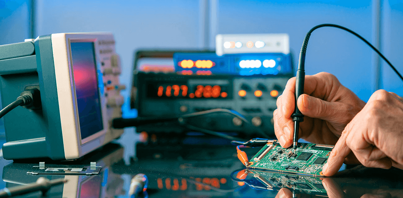
Board preparation and scanning. The sample is cleaned, and where potting, conformal coating or heavy oxidation is present, it is removed carefully. High resolution scans capture both surfaces and the inner layers if the board is delaminated or X-rayed. Layer extraction. Copper layers, solder mask, silkscreen and drill data are traced from the images, and for multilayer boards the inner layers have to be recovered by X-ray or by milling the board down layer by layer. Schematic capture. The netlist is derived from the copper and the component connections, then drawn as a readable schematic. BOM recovery. Every component is identified by marking, measurement or comparison, and a bill of materials is built with equivalents for obsolete parts. Layout reconstruction. The traced data is rebuilt in CAD, cleaned up to modern design rules where the customer allows it. Validation. A prototype is built and tested against the original.
Cost Drivers
Layer count. A two layer board can be traced from surface scans. A six or eight layer board needs X-ray or destructive milling, and the effort grows sharply with each inner layer. Board size and density. Trace count and via count set the tracing time, and a dense fine line board takes far longer than a simple one. Component identification. Parts with readable markings are easy; sanded, potted or house numbered parts require measurement, curve tracing and substitution research. Obsolete parts. Finding or replacing an end of life device can add days of engineering. Encapsulation. Potting, heavy conformal coating and embedded components make access difficult and risky. Output level. Delivering images only is cheap; delivering a validated schematic, a BOM and production ready Gerbers is not. Testing. Building and functionally testing a prototype is the step that proves the work, and it carries its own cost.
Typical Price Ranges in 2026
Absolute prices depend heavily on the board, so the useful way to think about it is by class. A simple two layer board with through-hole parts and clear markings sits at the low end, and can often be completed in a few engineering days. A four to six layer board with fine pitch SMD parts and some potted or unmarked components moves into the mid range, where X-ray work, curve tracing and obsolete part research dominate the time. A dense multilayer board, a high frequency board with controlled impedance, or a board with embedded components and no documentation can reach the top of the range, sometimes costing a significant fraction of the original design effort. In every class, the validation build and test is a fixed addition that does not scale down.
Legal and IP Considerations
Reverse engineering a board is a technical exercise with a legal dimension. The right approach is to confirm that you own the hardware or hold the rights to reproduce it, or that the work is limited to interoperability and repair in a way your jurisdiction permits. Keep a clear record of the purpose, the ownership of the sample and the deliverables. Reputable engineering firms will ask for that confirmation before starting, and a documented, legitimate purpose is also what makes the resulting design data defensible if it is ever questioned.
How to Reduce the Cost
Provide as much as you can with the sample: a working unit, a functional description, a partial schematic, a photograph of the silkscreen and any old documentation, however incomplete. A working board can be powered and probed, which saves guessing. If the board is potted, say so in advance, because removal method affects both price and risk. Decide what you actually need: if the goal is repair rather than production, a component level map and a BOM may be enough, and the full Gerber reconstruction is unnecessary. Finally, accept modernisation where possible: allowing a redesign to current design rules instead of an exact physical replica often lowers the cost and improves manufacturability.
Reverse engineering ends with a manufacturable design, so it should be handed to a fabricator who understands both the reconstruction and the build. Review how PCB manufacturing handles recreated data, align the reconstructed layout with workable PCB design and layout rules, and check the design and manufacturing considerations before release. A prototype PCB assembly run then proves the reconstruction matches the original in function.
FAQ
How long does PCB reverse engineering take? From a few days for a simple two layer board to several weeks for a dense multilayer or high frequency design.
What is the biggest cost driver? Layer count and component identification, because inner layers need X-ray or milling and unmarked parts need measurement and research.
Can a potted board be reverse engineered? Yes, but removing the potting adds risk and cost, and some damage to the sample should be expected.
Is reverse engineering legal? It depends on ownership and purpose. Work on boards you own or have the right to reproduce, and document the purpose with the engineering firm.
Conclusion
PCB reverse engineering cost is driven by how much of the design has to be recovered and how well the sample cooperates. Layer count, density, component identification and encapsulation set the engineering effort, while the validation build adds a fixed cost on top. Bring as much documentation and as many working samples as you can, decide whether you need repair data or full production files, and the project will land in a predictable range in 2026 instead of drifting.