
PCB Schematic vs PCB Design File: What Each Stage Defines
New engineers often use the terms interchangeably, and the confusion causes real mistakes: a review that treats a schematic as if it were a layout, or a change made in the layout that never finds its way back into the schematic. They are two distinct artefacts produced at two distinct stages, and understanding what each one defines is the basis for a controlled design flow.
What a PCB Schematic Is
A PCB schematic is a two-dimensional representation of the circuit. It shows the components and how they are connected, using agreed symbols, and it carries the values and the part numbers that will eventually appear in the bill of materials. It is a plan, or a blueprint, and it deliberately does not show where anything will be placed on the board.
Because it is drawn for legibility rather than for physical accuracy, a schematic has characteristics that would be impossible on a real board. Connections are not to scale. Nets cross each other freely, which cannot happen on a single copper layer. Signals that will be far apart on the board may be drawn adjacent, and signals on opposite sides of the board may be connected with a labelled link. Complex designs are often split into functional groups across several pages, which improves readability and makes the design easier to review.
What a PCB Design File Contains
The PCB design file is the physical realisation. It contains the board outline, the stackup, the component placement of every part with its actual footprint, the copper on each layer, the vias, the solder mask and the silkscreen. It is three-dimensional in the sense that height and layer position matter, and it is the artefact that goes to the fabricator and the assembler.
At this stage the constraints of the physical world apply. Two nets that must not connect have to be separated by routing around each other or by moving to a different layer. Trace widths have to satisfy both the current they will carry and the impedance they must present. Component spacing has to allow heat to escape, connectors have to sit at the board edge, and mechanical features have to match the enclosure. The silkscreen layer exists only here, and it is what allows an engineer or an inspector to identify components on the finished assembly.
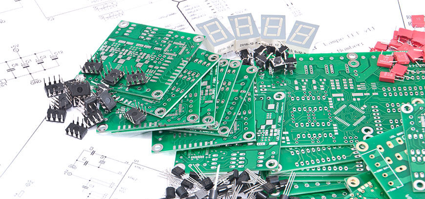
The two artefacts are linked by the netlist, and that link is what makes the flow controllable.
The Netlist as the Contract
The netlist is the machine-readable statement of connectivity that is exported from the schematic and imported into the layout. It is the contract between the two stages. Every component in the layout must correspond to a component in the schematic, every pad must belong to the correct net, and any change made in one place must be synchronised to the other.
When the two fall out of step, the consequences are subtle and expensive. A component added in the layout but not in the schematic will not appear in the bill of materials. A net renamed in the schematic but not re-imported leaves the layout routing a connection that no longer exists in the design intent. Regular synchronisation checks, and treating the netlist as a controlled document, prevent both.
Footprints and Pad Geometry
The layout stage is where the abstract symbol becomes a physical footprint, and the footprint is defined by the manufacturer drawing rather than by the symbol. Pad length, pad width, pitch, courtyard and the position of pin one all have to be verified against the datasheet. This is also where PCB pad design standards apply, because the pad geometry determines solderability, not just connectivity.
Footprint errors are the classic reason a board that worked in simulation cannot be assembled. A pad that is too short does not leave room for a fillet; a footprint whose courtyard is too small collides with its neighbour during placement. Because the layout is the first point at which these dimensions exist, verification belongs here rather than at the end of the project.
What Each Stage Decides
The schematic decides function: which components, connected how, with what values. The layout decides performance: how much impedance, how much coupling, how much heat, how much noise. A circuit that is correct on paper can be slow, noisy or unreliable in reality, and those outcomes are determined by the layout rather than by the schematic.
That division is worth stating explicitly in design reviews. Functional review checks the schematic against the requirements. Physical review checks the layout against the constraints, including current capacity, impedance targets, thermal paths and assembly requirements. Mixing the two into a single review usually means neither is done thoroughly.

The flow between the two stages is where projects most often lose time.
Working Between the Two
Layout frequently reveals a problem that requires a schematic change: a pin assignment that makes escape routing impossible, a regulator that cannot be placed where the thermal design requires, or a connector whose pinout conflicts with the mechanical design. When that happens, the change must be made in the schematic and re-imported, not patched in the layout.
Patching in the layout leaves the schematic describing a different circuit, and the next person to read it will be misled. If the change is genuinely layout-only, such as repositioning a decoupling capacitor, it does not require a schematic edit, although the placement and pad positioning consequences should still be reviewed. There is also a practical reason to keep the two in step: the bill of materials, the assembly data and the test documentation are all generated from the design database, and an inconsistency propagates into all of them.
From Design to Fabrication
When both stages are complete, the layout produces the manufacturing data: Gerber files for each copper and mask layer, a drill file, the stackup and the fabrication drawing, together with the assembly files. The PCB design and fabrication boundary is exactly here, and the quality of the handover depends on how disciplined the schematic-to-layout flow was in the preceding weeks.
A final design rule check on the finished database, followed by a review of the generated files rather than of the database, catches the remaining issues. The check verifies what the rules can express; the review verifies the intent that the rules cannot.
It is worth stating the sequence plainly. The schematic comes first, because it is where the circuit is designed and where mistakes are cheapest to fix. The layout follows, and it is where the circuit meets physics. Attempting to design the circuit in the layout, by adding components that were never in the schematic, reverses the flow and makes the design impossible to review.
FAQ
Can the schematic be changed after layout starts? It can and often must, but the change should be made in the schematic and re-imported into the layout. Editing the layout alone breaks the link between the two.
Why are schematic connections drawn on several pages? A complex design is easier to read when it is grouped by function. The layout does not follow that grouping, which is one reason the two artefacts look so different.
Which stage determines whether the board passes EMC? The layout. Emissions, coupling and return paths are physical properties, and they are decided by placement, stackup and routing rather than by the schematic.