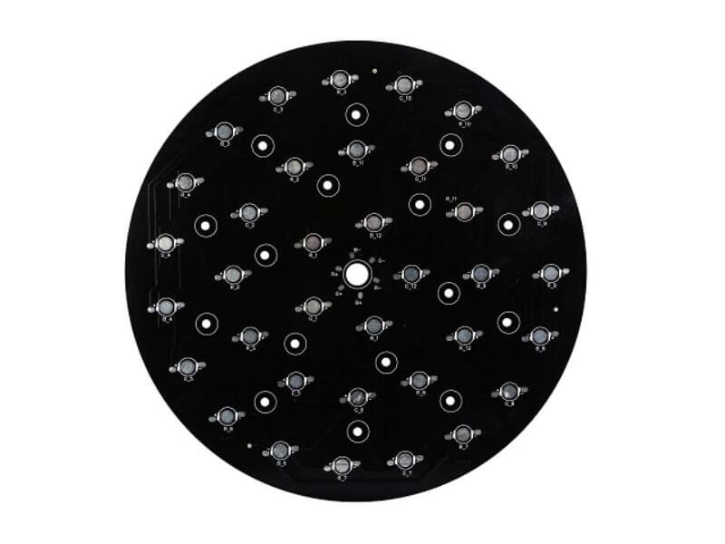
PCB Shipment Inspection to the IPC-A-600 Class 3 Standard
A customer who receives bare boards has no way to inspect the inside of a plated hole, and very little way to judge a surface finish beyond its appearance. That is why the acceptance standard has to be agreed before the boards are built rather than after they are delivered, and why the documents that travel with the shipment are as much a part of the product as the boards themselves.
The Standards Behind the Shipment
PCB shipment inspection at our factory is carried out against IPC-A-600 Class 3 for printed board acceptability, supported by an ISO 9001 quality system, IATF 16949 for automotive work and ISO 14001 for environmental management. RoHS compliance is treated as a baseline requirement rather than as an option that is added on request.
Class 3 is the class that matters for a product whose continued operation is essential. The consequence is that a number of conditions that would be accepted on a consumer board as a cosmetic observation become rejectable, and the inspection has to be able to detect them. The on-time delivery rate is maintained above ninety nine percent, and a single piece can be ordered, so the same standard applies to a prototype and to a production lot.
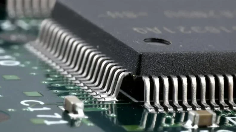
Appearance, Traces and Soldermask
Visual inspection is the widest net. The conductor pattern is checked for line width and spacing against the design, and for opens, shorts, nicks and burrs. The surface finish, whether immersion gold, hot air solder levelling or OSP, is judged for uniformity and for absence of oxidation, colour variation and missed plating.
Legend printing is checked for legibility, position and completeness, because a reference designator that is partly printed or in the wrong place turns into a rework instruction at the assembly line. The soldermask is examined for peeling, blistering, scratches and colour consistency. The board edge is examined for burrs, chipping and delamination, with the V-cut depth measured where the boards are to be separated rather than roughly assessed.
Electrical Verification
Continuity and isolation are verified on every order. Prototype and small volume lots go to a flying probe test, which needs no fixture and can therefore be applied to a design that will be built a few times. Volume orders use a dedicated test fixture, which is faster per board and gives better coverage of the network list.
Where the design specifies a controlled impedance, the value is verified with a time domain reflectometer and the result is available as a report. Boards that carry high voltage are given an additional dielectric strength test that is not part of the standard flow.
The point of separating these tests is that they answer different questions. A flying probe test proves that the netlist on the board matches the netlist in the data; an impedance measurement proves that the stack-up and the trace geometry produced the electrical property the designer intended. A board can pass the first and fail the second.
Dimensions, Registration and Warpage
The finished thickness, the outline dimensions and the hole diameter tolerances are measured against the drawing. Hole position is measured as an offset from nominal, and the quality of the plating inside the hole is part of the same check. For high density interconnect boards the layer to layer registration is verified and held within a tolerance of roughly twenty five micrometres.
Warpage is measured against the range allowed by the standard for the board thickness and the surface finish. A board that is flat in the panel and bows after separation is a common source of placement problems on the assembly line, and it is far cheaper to detect it at the fabricator than to discover it in the printer.

Sampling Reliability Checks
For volume orders and for orders with high reliability requirements, microsection analysis is added on a sampling basis. A cross section shows the copper thickness in the barrel, the dielectric thickness between layers and the alignment of the inner layers, which are exactly the properties that no external inspection can reveal.
The same sampling plan can include thermal stress testing, which shows how the board behaves at temperature, a solderability test on the pads, and adhesion testing of the soldermask and the legend. None of these is destructive in a way that affects the shipped quantity, because the samples are taken from the lot rather than from the customer’s boards.
Packing and the Documents That Travel
Inner packaging uses a vacuum bag inside an antistatic bag, so that moisture and dust are excluded. Boards are separated by glassine paper or pearl wool so that surfaces do not rub together, and the outer carton is reinforced at the corners to resist compression in transit. An inspection report covering the items tested and the results is included with every shipment.
Reports for flying probe testing, impedance measurement and microsection are available on request, and third party testing can be arranged where the customer’s own quality system requires it. Our PCB manufacturing flow produces the board, quality management holds the records, and the same order can continue into SMT assembly without the boards being packed and shipped in between.
Where the Emphasis Changes by Board Type
The standard is one document, but the items that decide acceptance differ with the board. On a high density interconnect board the blind and buried via connections, the layer to layer registration and the flatness of the resin filled vias carry the most weight, because those are the features a fault would hide inside. On a high frequency board the dielectric constant within a tolerance of about plus or minus nought point nought two five, the impedance accuracy and the insertion loss are the measurements that matter, and a board that is visually perfect can still be unusable.
On a high layer count board the lamination structure, the registration of the inner layer pattern, the aspect ratio of the holes and the insulation between layers are examined. On an aluminium backed board the thermal dielectric, the breakdown strength above four thousand volts and the thermal conductivity are the characteristics that decide whether the board will do its job. On heavy copper the uniformity of the copper thickness, the accuracy of the line width and the etch factor are the concerns, and on a rigid flex board the reliability of the bend area and the bond between the rigid and flexible sections are checked separately from the rest of the board.
Each product family therefore has its own inspection plan, and the plan records which measurements are made on every board and which are made on a sample. That distinction is what allows a report to be read correctly later: a value that was measured on every board and a value that was measured on one board out of the lot are not evidence of the same strength.
FAQ
What is the difference between Class 2 and Class 3? Class 3 rejects a number of conditions that Class 2 accepts, particularly where a defect could affect reliability rather than appearance, so the inspection and the documentation are stricter.
Which board types are covered? Rigid boards from one to thirty layers, HDI, high frequency material, aluminium backed, heavy copper and rigid flex, each with its own emphasis in the inspection plan.
Can fabrication and assembly be ordered together? Yes. Build the boards, then move them straight to the assembly line, which removes one packing cycle and one shipment from the schedule.