
Silkscreen Design Rules For PCB Assembly
The silkscreen, also called the legend, is the printed layer that carries component outlines, reference designators and polarity marks. It exists for the people who assemble, inspect and repair the board, and its rules are written to keep it readable without interfering with the soldering process.
A silkscreen design is therefore judged by two criteria at once. It has to be legible at the scale of the finished board, and it has to stay out of every area where solder will be applied, because ink on a pad prevents the joint from forming properly.
What The Legend Is For
The legend supports three activities: assembly, inspection and repair. During assembly it shows the operator where a part belongs; during inspection it links a defect to a designator; during repair it identifies a component without a schematic. A board with a poor legend costs time at every one of those stages.
It also carries information for the customer. A polarity mark, connector pin numbering and a board revision are usually printed rather than etched, because they have to be readable on the finished product rather than only in the design file.
Line Width And Text Height
The minimum line width for silkscreen is set by the printing process, and 0.15 mm is a common minimum with 0.2 mm preferred. Thinner lines break up during printing and produce a legend that is patchy and difficult to read under a microscope.
Text height is chosen from the space available. A common standard is 1.0 mm high characters with a stroke width of 0.15 mm, and 0.8 mm is used where space is tight. Below 0.6 mm the characters become difficult both for the printing process and for the human eye.
Reference Designator Placement
A reference designator should sit close to the component it identifies but outside the component body, so that it remains visible after assembly. Placing it under the part makes it useless once the board is populated, which is the most common silkscreen mistake.
The text should be oriented consistently, readable from one or two directions, and not rotated to fit into a corner. Consistency saves time during inspection, because the eye can follow a row of designators rather than searching for each one. The overall placement sequence is described under placement order and pad positioning.
Pad Clearance And Solder Mask
Silkscreen must be kept clear of pads. A printing process that deposits ink across a pad leaves a layer that the solder cannot displace, and the result is a joint with poor wetting or no joint at all. The usual clearance is 0.1 to 0.15 mm from the pad edge.

The clearance is measured to the pad, not to the solder mask opening. Because the mask opening is larger than the pad, a legend that is clear of the pad can still sit inside the mask opening and be printed on bare laminate, where adhesion is poor and the ink can flake off. The mask geometry behind this is described under PCB pad design standards.
Polarity And Pin One Marks
Polarity marks are as important as designators. A diode, an electrolytic capacitor or an integrated circuit must be oriented correctly, and the mark that shows the orientation has to be unambiguous and visible after assembly.
Pin one is normally marked with a dot beside the pad rather than a line across the corner of the body, because the body covers that corner once the part is fitted. A chamfered outline plus a dot is the clearest convention and is easy to check visually.
Common Errors
The errors that appear most often are legend text overlapping pads, designators hidden under components, and outlines drawn on top of a keepout area. All three are caused by treating the legend as decoration rather than as a functional layer of the design.
The other frequent problem is a legend copied from a reference design and never adjusted, leaving designators that do not match the parts and a polarity mark in the wrong place. How the legend is checked with the rest of the fabrication data is described under PCB design and fabrication.
Silkscreen And Solder Mask Openings
Silkscreen is printed after the solder mask, so the two layers interact directly. Ink that falls inside a mask opening sits on bare laminate or on exposed copper, where adhesion is much weaker than it is on cured mask. Over time, or during a washing or cleaning step, that ink can lift and leave a loose fragment sitting on the board.
The safe rule is to keep the legend outside the mask opening rather than merely outside the pad. A gap of about 0.15 mm from the mask edge is a practical figure, and it costs nothing because the space immediately around a pad is normally empty by design anyway.
Manufacturing Methods And Cost
Silkscreen is applied with a screen or with an inkjet process, and both have a resolution limit. Screen printing is cheaper at volume and produces a dense, opaque layer of ink, while inkjet is more flexible for small batches and needs no screen, though it gives a thinner and less opaque result.
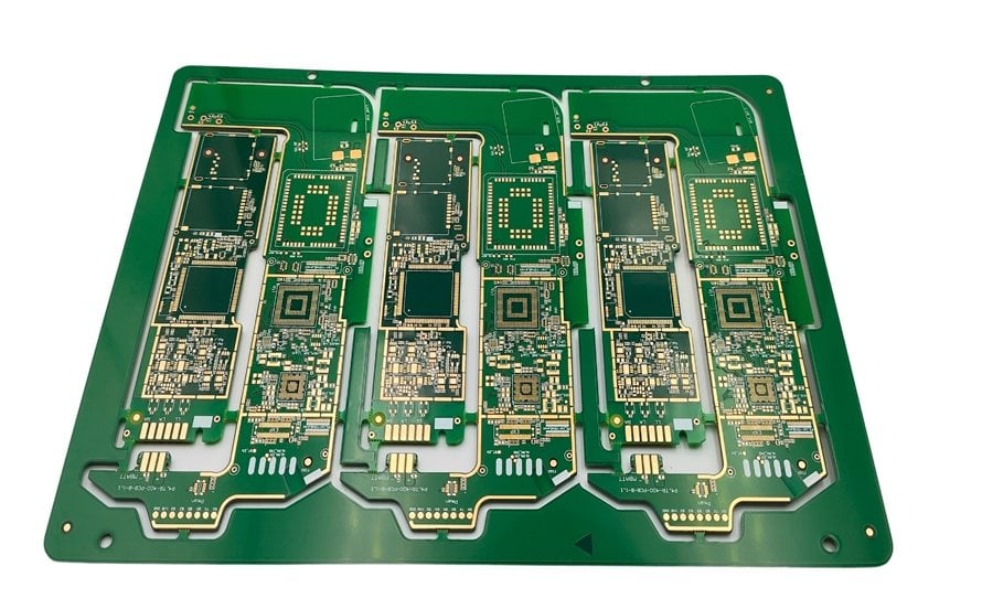
Including the legend costs almost nothing in the fabrication price, so there is no reason to remove it for economy. The only real cost is the engineering time needed to place the text correctly, and that time is repaid the first time a board has to be inspected or repaired on the line.
Checking The Legend Before Release
The legend should be reviewed with the same care as the copper. A useful check is to view the board at the scale at which it will be assembled, with component outlines turned on and copper turned off, and to look for text that is unreadable, overlapping or hidden behind a part.
A design rule check for silkscreen should flag text over pads, text over component bodies, and text below the minimum line width. Most layout tools include such a check, and it should be enabled at the start of a project rather than left to a visual review at the end.
Legend On Flex And Dense Boards
A flexible circuit tolerates only a limited amount of printed ink before its bending behaviour changes, and a dense legend on a flex layer can crack when the circuit is folded. The legend on a flex design is therefore kept minimal, and designators are often omitted entirely from the area that will bend.
On a very dense board the space between components is too small for readable text, so the legend is reduced to polarity marks and a handful of key designators. The remaining identification moves into the assembly drawing, which is acceptable as long as that drawing is available on the production line.
FAQ
Is silkscreen required on every board? Not always, but it is expected on anything that will be assembled or serviced. A board with no legend is difficult to inspect and impossible to repair without a drawing.
Can silkscreen be printed over a via? It should not be printed over an exposed via, because the ink can block the hole and contaminate the surface. A tented via under solder mask is not a problem.
What clearance is needed between legend and pads? Around 0.1 to 0.15 mm from the pad edge is the usual rule. The clearance should be checked against the solder mask opening as well as against the pad itself.