PCB Thermal and Electrical Separation Design in High Power LED Lighting
In high power LED lighting applications, the driving current of a single LED chip often reaches 350 mA to 1,500 mA or more. If junction temperature, or Tj, continuously exceeds 125 degrees Celsius, it will significantly accelerate lumen depreciation, reduce color coordinate stability, and shorten device life. Although traditional FR-4 double-sided PCB or ordinary metal core PCB can provide basic heat dissipation paths, the copper foil and aluminum substrate are bonded through thermal conductive adhesive. The electrical path and heat conduction path are highly coupled, meaning the positive and negative power traces and the thermal pad share the same copper layer. This makes it impossible to independently optimize thermal resistance, and electrical isolation margin is limited. PCB thermal and electrical separation, or TES, technology is exactly the key PCB design paradigm developed to break through this bottleneck. Its core is to decouple the high current power supply path from the high efficiency heat dissipation path in physical structure, achieving parallel and independent control of heat flow and current paths.
Structural Implementation Mechanism of PCB Thermal and Electrical Separation
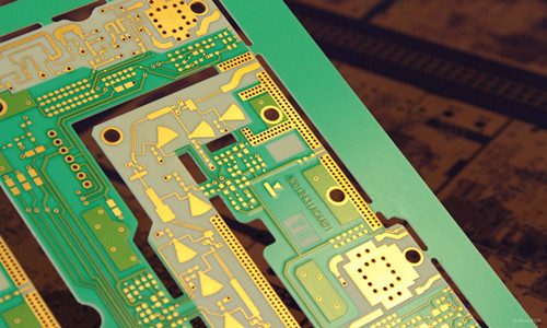
TES PCB usually uses a multilayer composite structure. The top layer is an independent power and signal routing layer formed by thick copper etching of 3 oz or more, that is, 105 micrometers or more. The bottom layer is pure heat dissipation copper foil of the same thickness or thicker, such as 4 to 6 oz, dedicated to connecting the thermal pad on the back of the LED pad. The middle layer embeds a high thermal conductivity insulating dielectric, such as AlN ceramic filler modified epoxy or boron nitride reinforced polyimide. Its thermal conductivity needs to reach 1.5 to 3.0 W per meter Kelvin, and breakdown strength must be greater than 8 kV per mm. The key is that there is no direct metal through-hole connection between the top copper and bottom copper. All electrical interconnections extend from the top layer to the middle signal layer through microvias or blind vias, and then are led out through independent traces. The bottom thick copper heat dissipation area is only pressed against the heat sink through thermal interface material, or TIM, forming a low resistance thermal channel. A 120 W street light module mass-produced by a certain international lighting manufacturer uses this PCB structure. The LED array is soldered on the top 3 oz copper, and the bottom 6 oz copper is fully covered and windowed. Measured thermal resistance from LED junction to housing, or Rth,j-c, is as low as 0.58 K per W, a reduction of 42 percent compared with a traditional metal core PCB of the same size.
Collaborative Design of Electrical Isolation and Safety Spacing
The PCB TES structure naturally strengthens high voltage isolation capability. Taking an LED module with 220 V AC input driven by PFC plus LLC topology as an example, the primary side high voltage area, such as the rectifier bridge output and PFC capacitor positive electrode, can all be laid out on the top thick copper. The secondary side low voltage LED loop is independently routed through the middle layer, and the bottom heat dissipation copper is completely floating. At this time, according to IEC 61347-1 and UL 8750 standards, creepage distance and electrical clearance are no longer constrained by the presence of the bottom copper. Because the bottom copper does not participate in electrical connection, its edge does not need to be included in the high voltage isolation boundary. In practice, designers can set an isolation slot of 8 mm or more between the top high voltage area and low voltage area. The slot is filled with solder mask green oil with dielectric strength of 100 V per micrometer or more. Combined with middle layer copper-clad grounding shielding, common mode noise suppression is improved by more than 15 dB. A certain industrial-grade mining lamp PCB uses this characteristic to achieve input-output isolation withstand voltage of AC 4000 V for 1 minute within a limited area of 28 mm by 32 mm, and EMI conduction test margin reaches 8 dB.

Thermal Path Modeling and Key Parameter Quantitative Verification
PCB TES performance evaluation must rely on three-dimensional thermal simulation and measured cross verification. A typical modeling process includes establishing in ANSYS Icepak or COMSOL a model containing real TIM contact thermal resistance measured at 0.15 to 0.35 square cm Kelvin per W, heat sink fin convection coefficient of 5 to 10 W per square meter Kelvin for natural convection, and LED transient thermal model obtained by T3Ster structural function testing. Focus on monitoring three node temperature differences. Delta T1 equals Tj minus Tsolder, reflecting LED package internal thermal resistance. Delta T2 equals Tsolder minus Tcopper_base, reflecting PCB TES insulating layer thermal conduction efficiency. Delta T3 equals Tcopper_base minus Theatsink, representing TIM and mechanical pressing quality. Measurements show that when the insulating layer thickness increases from 125 to 200 micrometers, delta T2 rises by about 18 percent. But if copper thickness is simultaneously increased from 3 oz to 4 oz, due to enhanced lateral heat diffusion, the overall Rth,j-c actually decreases by 3.2 percent. This reveals that PCB TES design is essentially a multi-parameter strongly coupled optimization problem, and a single variable cannot be adjusted in isolation.
PCB Manufacturing Process Challenges and Reliability Assurance Measures
PCB TES mass production faces three process difficulties. First, thick copper etching easily leads to excessive undercut, affecting line width precision and current carrying capacity. High resolution dry film plus pulse plating compensation must be used. Second, the CTE matching of high thermal conductivity insulating dielectric is crucial. The CTE of Al substrate is about 23 ppm per Kelvin, while the CTE of ceramic filler epoxy needs to be controlled at 18 to 22 ppm per Kelvin. Otherwise, interface delamination risk increases sharply during thermal cycling. Third, the flatness tolerance of the bottom thick copper must be 25 micrometers or less. Otherwise, a TIM contact void rate greater than 15 percent will deteriorate thermal resistance. A leading PCB factory improved copper-dielectric bonding force by introducing laser induced surface activation, or LISA, and used X-ray CT to perform full inspection of interface void rate on each batch of boards with AQL 0.65, ensuring that delivered PCB products still meet IPC-9708 Class 2 standard after 1,000 cycles from minus 40 to plus 85 degrees Celsius.
System-Level Thermal Management Collaborative Optimization Strategy
PCB TES is not an isolated solution. It needs deep collaboration with the system level. For example, in a constant current driving scheme, placing the current sampling resistor at the end of the top thick copper path rather than on the LED cathode side can prevent the sampling signal from being disturbed by heat dissipation copper temperature drift. In a multi-LED series architecture, connecting each LED thermal pad to the bottom copper through an independent thermal post rather than sharing a large pad can suppress thermal crosstalk. Measurements show that when the spacing between adjacent LEDs is less than 8 mm, if independent thermal posts are not used, the junction temperature rise of the rear LED can reach 1.7 times that of the front one. In addition, the bottom heat dissipation copper surface should be treated with matte black oxidation with emissivity greater than 0.85. In natural convection dominated scenarios, the radiation heat dissipation contribution can be increased by 22 percent. This is particularly critical for fanless applications such as sealed tunnel lights.
In summary, PCB thermal and electrical separation design has moved from high-end lighting prototypes to large-scale mass production. Its value lies not only in reducing thermal resistance but also in reconstructing the design logic of PCB as a thermal-electrical-mechanical multi-physics coupling carrier. Engineers need to abandon the traditional thinking of treating PCB as a passive wiring platform and instead regard it as the front-end execution unit of an active thermal management system. By precisely controlling material selection, stack-up definition, geometric topology, and process windows, every micrometer of copper thickness, every microwatt of heat consumption, and every volt of isolation voltage can achieve optimal balance under system target constraints. In the future, with the popularization of SiC drivers and the maturity of Mini and Micro LED transfer printing processes, PCB TES structures will further evolve toward higher integration, lower thermal resistance density of less than 0.3 K per W, and dynamic thermal reconfiguration.
Gopcba provides professional PCB manufacturing, PCB assembly, prototype PCB assembly, low-volume PCB assembly, high-volume PCB assembly, SMT PCB assembly, through-hole PCB assembly, mixed-technology PCB assembly, flex PCB assembly, PCB design layout, components procurement, rapid PCBA prototyping, conformal coating, PCBA testing, box build assembly, wire cable harness assembly, medical PCBA, telecommunications PCBA, energy PCBA, industrial PCBA, artificial intelligence PCBA, Internet of Things PCBA, PCB capabilities, and PCBA capabilities. You can also visit our blog, learn about us, see why us, review our quality management, or contact us for more information.