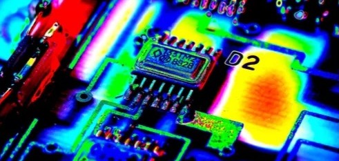
Electronic equipment inevitably generates heat during operation. As electrical current flows through components, copper traces, vias, power devices, and other structures, part of the electrical energy is converted into heat.
If this heat cannot be transferred away efficiently, the temperature of the PCB and surrounding components will gradually increase. Excessive temperature can affect electrical performance, accelerate component aging, reduce reliability, and in severe cases cause thermal failure.
For this reason, effective PCB Thermal Management is an important part of modern PCB Design.
As electronic products become smaller while power density continues to increase, thermal design is becoming increasingly important. High-power processors, power converters, MOSFETs, LEDs, motor drivers, RF power amplifiers, and other components can create localized hot spots that must be carefully managed.
What Causes PCB Heating?
PCB heating is primarily related to power dissipation.
The basic relationship is:
P = VI
where:
- P is electrical power,
- V is voltage,
- I is current.
For resistive elements, power loss can also be expressed as:
P = I²R
where R is resistance.
This means that even a relatively small resistance can generate considerable heat when a large current flows through it.
Heat may be generated by:
- Power semiconductors
- Voltage regulators
- DC/DC converters
- MOSFETs
- CPUs and processors
- LEDs
- RF power amplifiers
- High-current PCB traces
- Connectors
- Resistors
- Inductors
- Transformers
- Batteries and power-management circuits
The total thermal condition of a PCB is therefore determined not only by individual components but also by the overall power distribution and mechanical structure of the electronic system.
Why PCB Thermal Management Matters
Excessive temperature can affect both components and PCB materials.
Potential consequences include:
- Reduced component lifetime
- Electrical parameter drift
- Increased leakage current
- Reduced semiconductor reliability
- Solder-joint fatigue
- PCB warpage
- Delamination
- Accelerated aging
- Reduced system performance
- Thermal shutdown
- Permanent component failure
Temperature also affects reliability over time. In many electronic components, higher operating temperatures accelerate degradation mechanisms.
Therefore, PCB Thermal Management should be considered during the initial design stage rather than added after thermal problems appear in prototypes.
Main Heat-Transfer Paths in a PCB
Heat generated by an electronic component can be transferred through several paths.
1. Conduction Through the PCB
Heat can travel from the component into:
- Copper pads
- Copper traces
- Copper planes
- Thermal vias
- PCB dielectric layers
- Metal cores or heat-spreading structures
Copper has relatively high thermal conductivity compared with most PCB dielectric materials, so appropriately designed copper areas can help spread heat.
2. Conduction to a Heat Sink or Chassis
High-power components may transfer heat through a thermal interface into:
- Heat sinks
- Metal chassis
- Aluminum plates
- Copper spreaders
- Mechanical frames
The effectiveness of this path depends on the complete thermal resistance chain rather than simply the conductivity of one material.
3. Convection to Air
Heat can also be transferred from the PCB surface and components to the surrounding air.
This can occur through:
- Natural convection
- Forced-air cooling
- Fans
- Blowers
The effectiveness of convection depends on airflow, component geometry, temperature difference, enclosure design, and available surface area.
4. Radiation
At elevated temperatures, thermal radiation also contributes to heat transfer.
Although radiation may be less dominant than conduction and convection in many PCB applications, it can become relevant in systems with high surface temperatures or limited airflow.
PCB Cooling Methods
Different products require different cooling strategies.
A practical thermal solution may combine several approaches:
- PCB copper heat spreading
- Thermal vias
- Heat sinks
- Heat spreaders
- Thermal interface materials
- Natural convection
- Forced-air cooling
- Metal-core PCB structures
- Mechanical chassis conduction
- Active cooling systems for demanding applications
Therefore, it is not technically accurate to state that PCBs should always use active cooling or always use passive cooling. The appropriate method depends on power density, allowable temperature, enclosure structure, environmental conditions, component specifications, and system-level thermal requirements.
1. Use the PCB Itself as a Heat-Spreading Structure
The PCB can participate directly in heat spreading.
Large copper areas can distribute heat away from high-power components and reduce localized temperature concentration.
However, designers should consider copper thickness, copper area, layer structure, thermal vias, and the available heat-transfer path.
Simply increasing the copper area does not guarantee a proportional reduction in temperature.
The heat must ultimately reach a location where it can be transferred to the surrounding environment or a dedicated cooling structure.
2. Use Heat Sinks and Thermal Interface Materials
High-power components may require a dedicated heat sink.
A typical thermal path can be represented as:
Component → PCB Copper → Thermal Structure → Thermal Interface Material → Heat Sink/Chassis → Ambient
The thermal interface material should provide good contact between surfaces while minimizing thermal resistance.
Common materials include:
- Thermal pads
- Thermal grease
- Thermal gap fillers
- Electrically insulating thermal films
- Thermally conductive adhesives
Material selection should consider thermal conductivity, thickness, compression, electrical insulation, mechanical requirements, and long-term reliability.
3. Optimize PCB Layout for Heat Dissipation
PCB Layout has a major influence on temperature distribution.
High-power components should be placed where heat can be removed efficiently.
Important considerations include:
- Keep high-power components away from temperature-sensitive devices.
- Provide sufficient copper around heat-generating components.
- Use thermal vias where appropriate.
- Avoid concentrating multiple hot components in a small area.
- Maintain practical airflow channels.
- Place temperature-sensitive components in cooler regions.
- Consider the thermal path during component placement.
The objective is not simply to spread components uniformly. Instead, component placement should reflect power density, heat-transfer paths, electrical relationships, and mechanical constraints.
4. Position Temperature-Sensitive Components Carefully
Temperature-sensitive components should be kept away from major heat sources whenever practical.
Examples include:
- Precision voltage references
- Temperature sensors
- Crystal oscillators
- Precision analog circuits
- Low-noise amplifiers
- Battery-monitoring circuits
- High-accuracy measurement circuits
For example, placing a temperature sensor immediately next to a high-power MOSFET can cause the sensor to measure local heating rather than the actual ambient or target temperature.
Likewise, a precision voltage reference located near a switching regulator may experience thermal and electrical disturbances.
5. Study the Airflow Path
For air-cooled equipment, the airflow path is an important part of Thermal Management.
Designers should consider:
- Air inlet position
- Air outlet position
- Fan direction
- Component height
- Enclosure openings
- Heat sink orientation
- Internal obstructions
- PCB orientation
The cooling air should reach the major heat-generating components effectively rather than being blocked by mechanical structures.
In forced-air systems, the airflow path should be analyzed at the system level instead of focusing only on the PCB.
6. Avoid Concentrating Hot Spots
A PCB with several high-power components can develop multiple local hot spots.
If these devices are placed too close together, their thermal fields can overlap and create a significantly hotter region.
A better approach is to evaluate the total power density and thermal coupling of the area.
Where possible:
- Distribute high-power components appropriately.
- Provide adequate copper heat spreading.
- Maintain airflow access.
- Separate sensitive components from hot regions.
- Provide independent thermal paths for major heat sources.
This can produce a more uniform PCB temperature distribution.
7. Place High-Power Components Near Effective Cooling Paths
Components with high power dissipation should be positioned close to an effective thermal path.
Depending on the product structure, this may mean placing them near:
- Heat sinks
- Chassis walls
- Metal frames
- Thermal spreaders
- High-airflow regions
- Dedicated copper heat-spreading areas
The shortest electrical path is not necessarily the best thermal path. PCB Design should balance electrical performance, thermal performance, mechanical requirements, and manufacturability.
8. Consider PCB Orientation
For systems using natural convection, PCB orientation can influence airflow and temperature distribution.
Vertically oriented boards may allow warm air to rise naturally through the enclosure, depending on the mechanical structure.
Component placement should therefore consider the direction of natural convection.
However, orientation alone cannot compensate for excessive power density. If natural convection cannot remove the required amount of heat, additional thermal measures may be necessary.
9. Arrange Components According to Thermal Characteristics
Components can be divided into different thermal zones.
High-Heat Components
Examples include:
- Power transistors
- MOSFETs
- Switching regulators
- Power amplifiers
- High-power LEDs
These components should be placed where effective heat transfer is available.
Temperature-Sensitive Components
Examples include:
- Precision references
- Sensors
- Analog front ends
- Timing devices
These should generally be placed away from major thermal sources.
This type of thermal zoning should be coordinated with electrical partitioning.
10. Place High-Power Devices Near the Board Edge When Appropriate
For some PCB structures, placing high-power devices near the board edge can shorten the thermal path to a chassis, heat sink, or external cooling structure.
This can be particularly useful when the enclosure provides a direct mechanical heat-transfer path.
However, the board edge should not be treated as an automatically superior cooling location. The actual benefit depends on how the PCB connects to the mechanical cooling structure.
11. Reduce Thermal Resistance
Thermal performance is strongly influenced by thermal resistance.
The basic relationship can be expressed as:
Rθ = ΔT / P
where:
- Rθ is thermal resistance,
- ΔT is temperature difference,
- P is dissipated power.
Lower thermal resistance generally allows heat to move more efficiently from the component to the final heat sink or environment.
The complete thermal path should therefore be evaluated.
For example:
Junction → Package → PCB Copper → Thermal Via → Heat Spreader → Heat Sink → Ambient
A bottleneck anywhere in this chain can limit the effectiveness of the entire thermal solution.
12. Use Thermal Vias Where Appropriate
Thermal vias can transfer heat between PCB layers and help connect a component’s thermal pad to a larger copper structure.
They are particularly useful for packages with exposed thermal pads.
Depending on the design, thermal vias can connect the component pad to:
- Internal copper planes
- Bottom copper areas
- Heat-spreading structures
- Metal-core structures
Via diameter, pitch, plating, filling, and arrangement should be selected according to the component package and manufacturer’s manufacturing capability.
13. Copper Thickness and Thermal Performance
Copper thickness affects both electrical resistance and thermal spreading.
Increasing copper thickness can reduce resistance and improve the ability of a copper structure to distribute heat.
However, thicker copper also affects:
- Etching
- Line-width control
- Via plating
- Manufacturing tolerances
- PCB weight
- Cost
Therefore, copper thickness should be selected according to the combined electrical, thermal, mechanical, and manufacturing requirements.
14. Consider Metal-Core PCB Structures
For applications with high thermal requirements, a metal-core PCB may provide an alternative thermal path.
A typical metal-core structure may include:
Copper Circuit Layer → Dielectric Layer → Metal Core
The metal core, often aluminum or copper, can help spread heat toward a heat sink or chassis.
However, metal-core construction does not automatically solve all thermal problems.
The dielectric layer between the circuit copper and metal core remains an important part of the thermal path. Its thermal conductivity and thickness can strongly affect overall thermal resistance.
15. Thermal Design for High-Power PCB Applications
High-power applications require more comprehensive thermal planning.
Typical examples include:
- LED lighting
- Power supplies
- Motor controllers
- Battery management systems
- Automotive electronics
- Industrial power electronics
- Renewable-energy equipment
- RF power systems
In these applications, engineers should evaluate:
- Maximum component temperature
- Ambient temperature
- Power dissipation
- Thermal resistance
- Copper thickness
- Thermal vias
- Heat sink requirements
- Airflow
- Enclosure design
- Reliability requirements
Thermal simulation can also be used during development to identify potential hot spots before prototype testing.
16. PCB Heating and Reliability
Thermal design is directly related to product reliability.
Repeated temperature cycling can create mechanical stress because PCB materials, copper, components, solder joints, and mechanical structures have different coefficients of thermal expansion.
Long-term thermal stress may contribute to:
- Solder-joint fatigue
- Via reliability problems
- Component aging
- PCB delamination
- Warpage
- Electrical parameter drift
For high-reliability products, thermal cycling and temperature-rise testing should therefore be considered alongside normal electrical testing.
17. Thermal Testing and Verification
A thermal design should be verified using measurements.
Common methods include:
Thermocouples
Thermocouples can measure temperatures at selected component or PCB locations.
Infrared Thermal Imaging
Thermal cameras can provide a visual map of PCB temperature distribution and help identify hot spots.
Temperature Sensors
Embedded sensors can monitor temperature during operation.
Thermal Simulation
Simulation can estimate temperature distribution and identify potential thermal bottlenecks before hardware testing.
Actual measurements remain important because real products include variables that may not be fully represented in simulation, such as contact resistance, assembly variation, airflow changes, and component tolerances.
Common PCB Thermal Design Mistakes
Mistake 1: Focusing Only on the Heat Sink
A large heat sink cannot compensate for a poor thermal path between the component and the heat sink.
Mistake 2: Ignoring Hot Spots
Average PCB temperature may appear acceptable while individual components operate above their recommended temperature.
Mistake 3: Placing Sensitive Components Near Power Devices
Local heat can affect precision circuits and sensors.
Mistake 4: Ignoring Airflow
A fan cannot provide effective cooling if the enclosure prevents air from reaching the heat-generating components.
Mistake 5: Using Thermal Vias Without a Complete Thermal Path
Thermal vias can move heat between layers, but heat still needs an effective path to the final cooling structure.
Mistake 6: Increasing Copper Without Considering Manufacturing
Large copper areas and heavy copper structures can introduce manufacturing challenges and may not provide sufficient thermal improvement by themselves.
A Practical PCB Thermal Management Workflow
A practical thermal design process can follow these steps:
Step 1: Calculate Power Dissipation
Identify the major heat-generating components and estimate their power losses.
Step 2: Identify Temperature Limits
Determine the maximum allowable operating temperature for critical components.
Step 3: Create a Thermal Map
Identify hot zones and temperature-sensitive areas.
Step 4: Plan Component Placement
Separate major heat sources from sensitive components while maintaining required electrical relationships.
Step 5: Design the Thermal Path
Define the path from component to PCB copper, vias, heat spreader, heat sink, chassis, and ambient environment.
Step 6: Optimize PCB Layout
Use appropriate copper areas, thermal vias, copper thickness, and layer structures.
Step 7: Evaluate Airflow
Analyze natural or forced convection at the system level.
Step 8: Simulate and Test
Use thermal simulation where appropriate, followed by prototype temperature measurements.
Step 9: Optimize the Design
Adjust component placement, copper distribution, cooling structures, and airflow according to measured results.
Kingda’s Approach to PCB Thermal Management
At Kingda, thermal requirements can be considered together with electrical performance and manufacturing capability during PCB Design and production planning.
For boards with significant thermal requirements, important factors may include:
- Copper thickness
- Copper distribution
- Thermal vias
- High-power component placement
- Metal-core PCB structures
- PCB stackup
- Thermal interface requirements
- Surface finish
- PCB assembly
- Manufacturing tolerances
- DFM considerations
Kingda can work with customers to evaluate the relationship between PCB construction, component power dissipation, thermal paths, and manufacturing requirements.
For high-power and high-density designs, early thermal planning helps reduce the risk of hot spots, assembly problems, and reliability issues during later production stages.
Conclusion
Effective PCB Thermal Management is essential for electronic products with high power density, compact structures, and demanding reliability requirements.
PCB heating is influenced by electrical power dissipation, copper resistance, component characteristics, PCB construction, thermal paths, airflow, and mechanical design.
A successful thermal solution should therefore combine appropriate PCB Layout, copper heat spreading, thermal vias, heat sinks, thermal interface materials, airflow management, and system-level cooling where necessary.
Rather than relying on a single cooling method, designers should evaluate the complete path from the heat source to the final heat-rejection mechanism.
By considering PCB Heating, Heat Dissipation, Thermal Resistance, and Thermal Management from the earliest stages of PCB Design, manufacturers can achieve more stable operating temperatures, improved reliability, and better overall product performance.