PCB Traces: Structure, Materials and Design Rules
A trace is a copper conductor manufactured by etching away everything around it, and its shape is the whole of its electrical behaviour. Width, thickness, length and the distance to its reference plane determine resistance, inductance, impedance and how much it disturbs its neighbours.
How a Trace Is Formed
Traces are created by imaging a resist pattern onto copper-clad laminate, developing it and etching the unprotected copper away. The remaining conductor has a trapezoidal cross section rather than a rectangle, because the etchant attacks sideways as well as downwards, and that undercut is larger on thicker copper.
On inner layers the conductor is a foil bonded to the core. On outer layers the finished thickness includes the plating used to form the via barrels, so a design that starts with one ounce foil ends up closer to one and a half ounces after plating. Impedance and current calculations must use the finished value.
Materials and the Copper System
The conductor is copper because of its combination of conductivity, cost and manufacturability. Purity matters: foil and plating bath chemistry both affect resistivity, and a poorly controlled bath produces a deposit with higher resistance and poorer ductility.
Where a low-resistance path is needed, thickness is the practical lever. Where a low-adhesion surface is required, such as on a board that will be bent, a treated foil or a different surface preparation keeps the copper attached through mechanical stress.
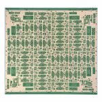
<img src="https://www.gopcba.com/wp-content/uploads/2026/06/Telecommunications-Electronics.jpg" alt="PCB traces etched on copper with controlled impedance geometry” />
Trace Width, Thickness and Resistance
Resistance is proportional to length and inversely proportional to cross-sectional area, so a trace can be made lower in resistance by widening it, thickening it or shortening it. Width is usually the cheapest option because it costs only board area, while thickness costs material and process time.
On a layer with a reference plane, increasing thickness has a second effect: it reduces the trace’s inductance as well. That is why heavy copper is common in power distribution, where the goal is both low resistance and low impedance at the switching frequency.
Current Capacity and Temperature Rise
Current capacity is a thermal question rather than a purely electrical one. A trace heats because of its resistance, and its temperature stabilises where the heat generated equals the heat removed by conduction into the board and convection from the surface.
The practical implication is that the same trace can carry more current on an inner layer, where the copper planes conduct heat away, than on an outer layer in still air. The calculation method matters less than using one consistently and applying margin, and the reference approach is the trace width and current calculation covered elsewhere.

Controlled Impedance Traces
A trace becomes a transmission line when its length is a significant fraction of the signal wavelength. At that point its impedance is set by its width, the dielectric thickness beneath it and the dielectric constant, and it must be held constant along its length.
Two standard geometries dominate. A microstrip runs on an outer layer above a reference plane and is exposed to air, while a stripline is buried between two planes and is fully embedded in dielectric. The choice affects both the achievable impedance range and the susceptibility to crosstalk, as discussed in the comparison of microstrip and stripline routing.
Spacing and Crosstalk
Two nearby traces couple through the electric and magnetic fields between them. The coupling rises as the spacing shrinks and as the parallel run lengthens, and it becomes significant when traces run side by side for a long distance on the same layer.
The 3W rule is a useful default: keeping the centre-to-centre spacing at least three times the trace width reduces coupling to a manageable level for most digital signals. Where a design must run traces closer, adding a ground trace between them or moving one to another layer with a plane in between is more effective, and the 3W spacing rule is worth reviewing before reducing spacing.
Length Matching and Timing
Signals travel along a trace at a speed that depends on the dielectric, typically around half the speed of light in vacuum for a board-mounted microstrip. At that speed, one hundred millimetres of trace is roughly six hundred picoseconds of delay, which is significant for parallel buses and differential pairs.
Length matching compensates for the difference in arrival time between related signals. It is only meaningful for signals that must arrive together, and matching everything on general principle adds serpentine routing that wastes area and creates its own coupling, which is why the serpentine and length matching rules are worth following rather than improvising.
Vias, Layer Changes and Return Paths
Every layer change introduces a via with its own capacitance and inductance, and it interrupts the reference plane that the trace was using. The return current has to find a path across the layer change, and if no ground via is provided nearby, it will find a longer and more disruptive route.
The practical rule is to place a ground via beside every signal via on a high-speed net and to keep the layer change short. Where a return path cannot be continuous, the discontinuity should be placed at a point in the channel where it does the least harm rather than at random.
Design Rules That Prevent Rework
Set the design rules from the fabricator’s capability rather than from the tool default, and apply them consistently across the project. Verify the minimum width and spacing against the copper weight, since a rule written for one ounce copper will not hold on three.
Then review the routing with the fabrication constraints in mind. Acute angles concentrate etchant and produce narrow necks, small isolated copper features lift during processing and traces too close to the board edge are exposed during routing. These are inexpensive to fix in the layout and expensive to fix afterwards.
Traces, Test Points and Probing
A trace that cannot be probed is a trace that cannot be debugged. Adding a small test pad on a net costs almost nothing at layout time and saves hours during bring-up, particularly on power rails and on any net that crosses a boundary between functional blocks.
Test points should be placed where a probe can reach them without shorting a neighbouring pad, which means keeping them away from fine-pitch components and giving them enough clearance for the probe tip. Where a bed-of-nails fixture will be used in production, the test points additionally need to sit on a consistent grid and be clear of tall components.
A short stub to a test pad is harmless on a slow net and harmful on a fast one, because the stub becomes a resonator. On high-speed nets the test pad should sit in line with the trace rather than on a spur, or the net should be tested through a via that is already part of the routing.
FAQ
Does trace shape affect signal quality? It does, mainly through impedance and through discontinuities such as vias and stubs. A trace that holds its geometry keeps its impedance, while a neck or an abrupt change creates a reflection.
How wide should a power trace be? Wide enough to carry the current within the temperature rise the product allows, which is usually determined by the copper weight and the available area rather than by a fixed number. A short wide trace on an inner layer outperforms a long narrow one on an outer layer.
Can traces be routed at any angle? Any angle is manufacturable, but 45 degree segments are preferred because they keep the conductor width consistent and avoid the etchant trapping that occurs at very acute angles.