PCB Traces, Through Vias, Blind Vias and Buried Vias Explained
In modern electronic systems, a PCB serves as a precision platform for electrical interconnection, signal transmission, power distribution, and component integration. Although a circuit board may appear to be a simple flat structure, its internal electrical network can be highly complex.
Two fundamental elements make this electrical network possible: conductive PCB traces and interconnection holes known as vias. Traces provide horizontal electrical paths within individual PCB layers, while vias create vertical connections between different layers.
As electronic products become smaller and more functionally integrated, multilayer circuit boards increasingly rely on advanced interconnection structures. Understanding the differences between through vias, blind vias, and buried vias is therefore important for PCB designers, engineers, and electronics manufacturers.
What Are PCB Traces?
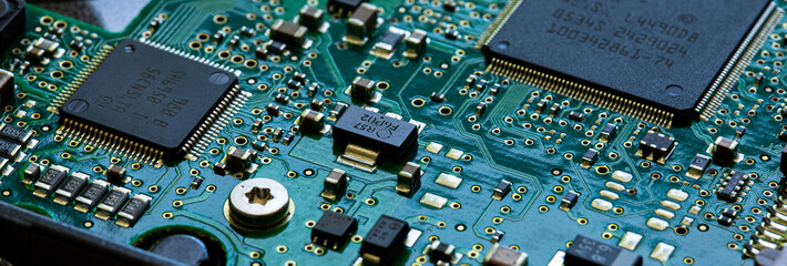
PCB traces are conductive paths formed on the surface or internal layers of a printed circuit board. They are typically manufactured from copper and provide electrical connections between components, pads, vias, connectors, and other conductive structures.
Unlike conventional wires, PCB traces are integrated directly into the board structure. Their width, thickness, spacing, geometry, and routing direction are determined according to electrical, mechanical, thermal, and manufacturing requirements.
For example, a power circuit carrying relatively high current may require wider or thicker copper traces to reduce resistance and temperature rise. In contrast, high-speed digital or RF signals may require carefully controlled trace geometry, spacing, impedance, and reference planes.
The Main Functions of PCB Traces
PCB traces perform several essential functions:
- Carry electrical current between components
- Transmit digital and analog signals
- Connect different functional areas of a circuit
- Provide power and ground distribution
- Form controlled-impedance transmission lines
- Work with vias to establish three-dimensional electrical connections
The layout of traces can have a direct effect on electrical performance. Poor routing may increase electromagnetic interference, crosstalk, signal reflection, voltage drop, and other electrical problems.
For complex boards, professional PCB Manufacturing capabilities are important because trace geometry must remain consistent with the original design throughout imaging, etching, lamination, plating, and inspection.
What Are Vias on a PCB?
While traces primarily provide electrical connections within a PCB layer, vias provide electrical connections between different layers.
A via is a plated hole that creates a conductive path between selected copper layers. Depending on its construction and connection range, a via can be classified as a through via, blind via, or buried via.
These structures are particularly important in a multilayer PCB, where multiple conductive layers are separated by insulating dielectric materials.
Through Vias: Full-Depth Interconnection
Through vias are one of the most common via structures used in conventional multilayer circuit boards.
A through via extends from the top surface of the PCB to the bottom surface, passing through the complete board thickness. Its hole wall is plated with copper, allowing electrical connections to be established between different conductive layers.
Because the hole passes through the entire board, a through via can connect multiple PCB layers along its path.
Advantages of Through Vias
Through vias offer several practical advantages:
- Relatively straightforward manufacturing
- Reliable electrical interconnection
- Suitable for conventional multilayer PCB structures
- Compatible with a wide range of component and routing requirements
- Generally lower manufacturing complexity than advanced via structures
However, a through via also occupies routing space on every layer through which it passes. As PCB density increases, this can become a significant design limitation.
For high-density layouts, engineers may therefore consider HDI PCB technology, which can use microvias, blind vias, buried vias, fine-line routing, and sequential lamination to increase routing density.
Blind Vias: Surface-to-Internal-Layer Connections
Blind vias connect an outer PCB layer to one or more internal layers without extending through the entire board.
A blind via may begin on the top surface and terminate at a specified internal layer, or it may begin on the bottom surface and extend upward to an internal layer.
For example, a blind via can connect Layer 1 to Layer 2 or Layer 3 without occupying the complete vertical space of the PCB.
Why Are Blind Vias Used?
Blind vias are particularly useful when PCB designers need to increase routing density in a limited board area.
They can help:
- Free routing space on internal layers
- Improve component breakout
- Support fine-pitch BGA packages
- Reduce unnecessary through-hole structures
- Increase interconnection density
- Enable more compact PCB layouts
Blind vias are therefore widely associated with high-density interconnect designs.
In advanced applications, laser-drilled microvias can provide very small interconnections between adjacent layers. This allows designers to create shorter electrical paths while maximizing the available routing area.
Buried Vias: Internal-Layer Connections
Buried vias are completely contained within the internal structure of a PCB. They connect two or more internal conductive layers without reaching either the top or bottom surface.
Because they are embedded inside the board, buried vias cannot be directly seen from the external surfaces.
For example, a buried via may connect an internal Layer 3 to Layer 5 while remaining completely isolated from the external surfaces.
Benefits of Buried Vias
Buried vias can provide additional routing flexibility in complex multilayer designs.
Their main benefits include:
- Conserving valuable surface routing space
- Increasing internal-layer interconnection options
- Supporting high-density PCB architectures
- Reducing routing limitations caused by conventional through vias
- Enabling more compact multilayer designs
However, buried vias require additional manufacturing processes because the internal connections must be created before the complete PCB stack-up is assembled.
Therefore, they should generally be used when their routing or electrical advantages justify the additional manufacturing complexity.
PCB Traces vs. Through, Blind and Buried Vias
Although traces and vias work together, they serve different functions within a PCB.
| Structure | Main Function | Typical Connection |
|---|---|---|
| PCB traces | Horizontal electrical routing | Within the same layer |
| Through vias | Vertical electrical interconnection | Top-to-bottom through the board |
| Blind vias | Surface-to-internal connection | Outer layer to selected inner layer |
| Buried vias | Internal-layer connection | One inner layer to another |
| Microvias | High-density interconnection | Usually adjacent or closely spaced layers |
The major difference is therefore the direction and extent of electrical connection.
Traces primarily route signals and current across a PCB layer, while vias establish electrical paths between layers.
How Vias Affect Multilayer PCB Design
In a multilayer PCB, via selection is closely related to stack-up architecture, routing density, component packaging, signal integrity, and manufacturing capability.
A simple multilayer board may rely primarily on through vias. However, more complex boards may combine through vias with blind vias, buried vias, and microvias.
For example, a high-density BGA package may require blind microvias to escape signals from fine-pitch pads efficiently. Meanwhile, internal signal layers may use buried vias to create additional routing paths without consuming valuable surface area.
Via Placement and Spacing
Via placement must also be carefully controlled.
If vias are positioned too close to each other, traces, pads, or copper areas, the design may exceed manufacturing capabilities. This can create challenges involving drilling, layer registration, copper plating, and fabrication yield.
Proper multilayer PCB via spacing should therefore be evaluated during PCB layout rather than after the design is completed.
Engineers should consider:
- Via-to-via spacing
- Via-to-trace clearance
- Via-to-pad clearance
- Annular ring requirements
- Drill diameter
- Layer registration
- Copper thickness
- Manufacturing tolerances
Early design-for-manufacturing review can help identify these potential problems before production.
The Relationship Between Vias and Signal Integrity
Vias are not simply mechanical holes. They can also influence high-speed electrical performance.
When a high-speed signal changes layers through a via, the via structure can introduce discontinuities in the transmission path. Depending on the design, these discontinuities may contribute to impedance changes, reflections, crosstalk, or electromagnetic radiation.
For high-speed designs, engineers should therefore evaluate:
- Via geometry
- Pad size
- Anti-pad dimensions
- Signal reference planes
- Return-current paths
- Via stub length
- Differential-pair routing
- Layer transitions
For particularly demanding applications, high-speed and high-frequency PCB manufacturing requires coordinated stack-up engineering, material selection, impedance control, and fabrication-process control.
Choosing the Right Via Structure
The appropriate via structure depends on the PCB’s electrical, mechanical, and manufacturing requirements.
When to Use Through Vias
Through vias are generally suitable when:
- Board density is moderate
- Manufacturing cost is a major consideration
- Routing space is sufficient
- Conventional multilayer construction meets the design requirements
When to Use Blind Vias
Blind vias are useful when:
- Routing density is high
- Fine-pitch components require additional breakout space
- Surface-to-inner-layer connections are needed
- Designers need to reduce the routing space occupied by through vias
When to Use Buried Vias
Buried vias may be appropriate when:
- Internal-layer routing is highly complex
- Surface routing space is limited
- The PCB has a high layer count
- Additional internal interconnections are required
For advanced applications, the selection of blind and buried structures should be evaluated together with stack-up design, lamination processes, drilling capabilities, and manufacturing tolerances.
Manufacturing Considerations for Advanced PCB Via Structures
The transition from PCB design to manufacturing is critical for complex via structures.
Manufacturers must control processes such as:
- Inner-layer circuit fabrication
- Layer alignment
- Lamination
- Mechanical drilling
- Laser drilling
- Copper plating
- Via filling when required
- Outer-layer circuit formation
- Surface finishing
- Electrical testing and final inspection
For example, via filling may be required in certain HDI and via-in-pad applications. Proper filling can help create a more stable surface for component assembly and subsequent manufacturing processes. Poor filling may result in voids, cracks, surface depressions, or other defects.
For complex circuit boards, choosing a manufacturer with comprehensive PCB manufacturing capabilities can help ensure that the design intent is compatible with actual production processes.
Applications of Through, Blind and Buried Vias
Different via technologies are used across many electronic applications.
Consumer Electronics
Compact consumer devices often require high-density routing and miniaturized component packaging. Blind vias and microvias can help designers reduce PCB size while maintaining routing capacity.
Automotive Electronics
Automotive control units, ADAS systems, radar modules, battery management systems, and other electronic systems may require multilayer and HDI structures. High-density interconnect technologies can provide additional routing capacity within limited space.
Telecommunications and 5G
High-speed communication equipment may require controlled impedance, high-frequency materials, dense routing, and advanced via structures. Blind and buried vias can help optimize routing in compact communication hardware.
AI and High-Performance Computing
AI servers, processors, networking equipment, and other high-performance systems can require high-layer-count PCBs with complex power and signal-routing architectures.
In these designs, via structures must be considered together with signal integrity, power integrity, thermal management, and manufacturing capability.
How PCB Traces and Vias Work Together
A PCB is essentially a three-dimensional electrical network.
PCB traces provide horizontal routing paths across individual layers, while vias provide vertical transitions between layers. When these structures are combined, engineers can route signals and power through complex multilayer architectures.
A typical signal path may look like:
Component Pad → PCB Trace → Via → Inner-Layer Trace → Via → PCB Trace → Component Pad
This combination allows modern circuit boards to achieve high routing density without requiring every connection to remain on a single layer.
As electronic systems become increasingly compact and complex, the interaction between traces, vias, layer stack-up, materials, and manufacturing processes becomes increasingly important.
Conclusion
PCB traces, through vias, blind vias, and buried vias are fundamental elements of modern printed circuit board architecture.
PCB traces provide conductive paths within individual layers, while through vias create full-depth connections across the board. Blind vias connect external layers to selected internal layers, and buried vias establish connections entirely within the internal PCB structure.
The right combination depends on board density, electrical performance, component packaging, layer count, signal requirements, mechanical constraints, and manufacturing capabilities.
For high-density and advanced electronic products, early cooperation between PCB designers and manufacturers is especially important. Reviewing stack-up configuration, via structures, spacing, impedance, drilling requirements, lamination, and manufacturability before production can reduce redesign risk and improve manufacturing reliability.
With appropriate design rules and manufacturing processes, these interconnection technologies allow modern PCBs to achieve greater density, better electrical performance, and more efficient use of limited board space.