Lightweight Medical PCB Manufacturing for Portable Medical Devices
As medical technology continues to move toward portability, mobility, and compact integration, portable medical devices are becoming increasingly important in modern healthcare. From emergency medical equipment and bedside monitoring systems to home healthcare products and wearable medical electronics, portable devices make healthcare services more accessible and convenient.
As one of the most important electronic components inside these products, the PCB directly affects the device’s size, weight, electrical performance, battery life, and overall reliability. For this reason, Lightweight Medical PCB manufacturing has become an important technology for developing smaller, lighter, and more user-friendly medical electronics.
Unlike conventional PCB production, lightweight PCB manufacturing must achieve a careful balance between weight reduction, structural strength, electrical performance, thermal management, and long-term reliability. Material selection, circuit layout, board thickness, manufacturing processes, and quality control must all be considered together.
For medical device manufacturers, choosing the right Portable Medical Device PCB solution can help reduce equipment weight while maintaining the electrical and mechanical performance required for demanding healthcare applications.
1. The Core Objective of Lightweight Medical PCB Manufacturing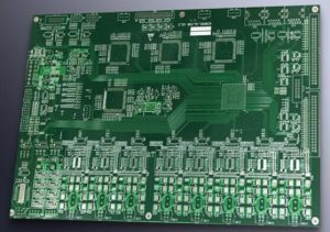
The primary goal of lightweight PCB manufacturing is not simply to make the circuit board thinner or smaller. Instead, the objective is to reduce weight and occupied space while maintaining the performance and reliability required by the final medical device.
Medical electronics often have strict requirements for electrical stability, signal integrity, insulation, mechanical strength, thermal performance, and long-term reliability. Any attempt to reduce PCB weight must therefore be carefully evaluated against these requirements.
A successful lightweight PCB design should consider several factors simultaneously:
- PCB material density
- Board thickness
- Layer count
- Copper thickness
- Component density
- Circuit routing
- Mechanical structure
- Thermal management
- Electrical insulation
- Manufacturing tolerances
The result should be a PCB that provides the required functionality without introducing unnecessary material, weight, or mechanical complexity.
GOPCBA provides advanced PCB Manufacturing capabilities for applications requiring multilayer, HDI, high-TG, flexible, rigid-flex, high-frequency, heavy-copper, and other specialized PCB structures. This range of manufacturing technologies gives engineers greater flexibility when optimizing PCB size and weight. (GOPCBA PCB Manufacturing)
2. Material Innovation: The Foundation of Lightweight PCB Design
Material selection is one of the most important factors in lightweight PCB development.
Traditional PCB structures generally rely on rigid FR-4 materials because of their good electrical insulation, mechanical strength, thermal stability, and cost-effectiveness. However, portable medical devices may require more specialized material solutions when weight and space are critical design constraints.
Lightweight and High-Performance Materials
Advanced PCB materials can help engineers reduce board thickness or overall weight while maintaining the mechanical and electrical properties required by the application.
Depending on the device structure, engineers may evaluate:
- Thin FR-4 materials
- High-TG materials
- Flexible PCB materials
- Rigid-flex materials
- High-performance laminates
- Specialized lightweight substrates
Flexible and rigid-flex PCB technologies can be particularly useful for compact medical products because they allow electrical connections to conform to limited or irregular spaces.
For example, a rigid-flex structure may replace multiple rigid boards and conventional cable connections, reducing both assembly space and unnecessary interconnection components.
GOPCBA’s published PCB capabilities include FR-4, high-TG FR-4, Rogers materials, aluminum substrates, flexible materials, and rigid-flex PCB technologies, allowing material selection to be matched to specific application requirements. (GOPCBA PCB Capabilities)
3. Design Optimization: Reducing Weight Without Sacrificing Performance
Material selection alone cannot achieve effective PCB weight reduction. PCB design and engineering optimization are equally important.
Optimizing Board Thickness
Reducing PCB thickness is one of the most direct approaches to reducing weight.
However, simply making the board thinner may reduce mechanical strength or create manufacturing and assembly challenges. Therefore, the final board thickness should be determined according to the application’s mechanical requirements, layer structure, component loading, and manufacturing capabilities.
A well-designed thin PCB should maintain sufficient rigidity and dimensional stability during assembly and operation.
Optimizing Copper Distribution
Copper is essential for electrical conduction, power distribution, grounding, thermal management, and signal transmission. However, unnecessary copper can increase PCB weight.
Engineers can optimize copper distribution by reviewing:
- Trace widths
- Copper thickness
- Ground planes
- Power planes
- Copper pours
- High-current areas
- Thermal structures
The goal is not to minimize copper indiscriminately, but to place copper where it is functionally required while avoiding unnecessary material.
Optimizing Layer Structure
Multilayer PCB technology allows designers to achieve high circuit density within a compact physical area.
Instead of increasing the physical size of a board to accommodate more circuits, engineers can use additional layers to integrate routing, power, and ground structures vertically.
This can be especially valuable for portable medical equipment where PCB footprint and enclosure size are limited.
For advanced medical applications, GOPCBA supports multilayer PCB, HDI, flexible, rigid-flex, high-TG, high-frequency, and controlled-impedance technologies. These technologies can help engineers achieve higher circuit density while maintaining electrical and mechanical performance.
4. Manufacturing Process Optimization for Lightweight PCBs
In addition to materials and design, manufacturing process optimization plays an important role in lightweight PCB production.
Precision Material Cutting
Accurate material cutting can reduce unnecessary substrate waste while maintaining dimensional accuracy.
During production, manufacturing engineers need to ensure that the selected panelization method makes efficient use of the raw material. Proper nesting and panel utilization can reduce waste and improve manufacturing efficiency.
Precision Drilling and Routing
Drilling and routing processes must be carefully controlled for thin and lightweight PCBs.
Excessive mechanical stress during drilling or routing may cause deformation, burrs, cracking, or dimensional instability.
Advanced manufacturing equipment and appropriate process parameters can help maintain consistent hole quality and board dimensions.
Controlled Lamination
For multilayer lightweight PCBs, lamination is a critical process.
The bonding between copper layers, prepreg, and core materials must remain stable while controlling board thickness and dimensional accuracy.
Poor lamination control may result in:
- Delamination
- Voids
- Resin starvation
- Board warpage
- Layer misalignment
- Mechanical instability
Therefore, lightweight multilayer PCBs require the same level of process discipline as conventional high-reliability circuit boards.
5. Flexible and Rigid-Flex PCBs for Portable Medical Devices
As portable medical equipment becomes smaller and more ergonomic, flexible and rigid-flex PCB technologies are becoming increasingly useful.
Flexible PCB Applications
Flexible PCBs can bend or fold within defined mechanical limits, allowing them to fit into compact or curved product structures.
They can be used in:
- Wearable medical devices
- Portable monitoring equipment
- Handheld diagnostic devices
- Medical sensors
- Patient monitoring systems
- Compact healthcare electronics
By replacing conventional wires, connectors, and multiple rigid boards, flexible circuits can potentially reduce assembly volume and overall system weight.
Rigid-Flex PCB Integration
Rigid-flex PCBs combine rigid board sections with flexible interconnections.
This structure can reduce the number of separate components required for internal electrical connections while improving mechanical integration.
For portable medical equipment, rigid-flex technology can help engineers create more compact internal architectures and improve reliability by reducing connector and cable interfaces.
GOPCBA supports flexible and rigid-flex PCB manufacturing as part of its advanced PCB capabilities, making these technologies suitable options for compact electronic designs. (GOPCBA PCB Capabilities)
6. Lightweight PCB Manufacturing for Medical Applications
Different portable medical devices have different requirements for PCB size, weight, electrical performance, and mechanical reliability.
Emergency Medical Equipment
Emergency equipment must often be transported quickly and operated in demanding environments.
Reducing PCB weight can contribute to lighter overall equipment, making portable diagnostic and monitoring systems easier for medical professionals to carry and deploy.
However, weight reduction must not compromise electrical stability or mechanical durability.
Home Healthcare Equipment
Home healthcare products are increasingly designed for easy operation and convenient long-term use.
Compact blood pressure monitors, portable diagnostic devices, home monitoring systems, and other healthcare products can benefit from smaller and lighter PCB structures.
A well-designed Medical PCB Design can help reduce internal space requirements while maintaining the electrical functionality required by the device.
Wearable Medical Electronics
Wearable medical electronics have particularly demanding weight and size requirements because the device may remain in direct contact with the user’s body for extended periods.
For these products, every component contributes to the overall user experience.
Lightweight flexible or rigid-flex PCBs can help reduce the weight and thickness of the electronic system while allowing the circuit to conform to the mechanical structure of the wearable product.
7. Quality and Reliability: The Non-Negotiable Requirement
Lightweight PCB manufacturing should never become a simple pursuit of minimum weight.
Medical electronics require stable performance because PCB failures can affect monitoring, measurement, communication, power management, or other critical device functions.
Therefore, Medical PCB Manufacturing must maintain strict quality controls throughout the entire production process.
Material Inspection
Incoming materials should be checked for:
- Material specification
- Thickness
- Copper foil thickness
- Surface condition
- Dimensional stability
- Electrical properties
- Material certification
Only qualified materials should enter production.
In-Process Inspection
During PCB manufacturing, critical process parameters should be monitored continuously.
Typical inspection items include:
- Board thickness
- Layer registration
- Hole dimensions
- Copper thickness
- Trace geometry
- Surface condition
- Warpage
- Solder mask quality
Early detection of process deviations can help prevent defective products from progressing to later manufacturing stages.
Electrical Testing
Electrical testing is particularly important for medical PCB applications.
Testing can identify potential:
- Open circuits
- Short circuits
- Connectivity problems
- Insulation problems
- Manufacturing defects
GOPCBA’s published quality management information states that PCB production includes strict process controls and 100% electrical testing, alongside incoming material inspection and manufacturing quality control. (GOPCBA Quality Management)
8. PCB Assembly Considerations for Lightweight Medical Devices
PCB weight reduction should also consider the components and assembly process.
A lightweight bare PCB can still become relatively heavy after component installation if component selection and placement are not optimized.
Therefore, the PCB and PCBA should be considered as a complete system.
Important factors include:
- Component size
- Component package type
- Component density
- Connector selection
- SMT versus through-hole assembly
- Thermal requirements
- Mechanical support
- Assembly space
For highly compact medical devices, SMT technology can help increase component density while reducing the space required by conventional through-hole components.
GOPCBA provides PCB assembly capabilities including SMT, through-hole, mixed-technology, prototype, low-volume, high-volume, and turnkey PCB assembly. (GOPCBA PCBA Capabilities)
9. Balancing Lightweight Design With Thermal Management
One of the challenges of lightweight medical PCB design is maintaining sufficient thermal performance.
Reducing material volume may affect the board’s ability to dissipate heat, particularly when the PCB contains processors, wireless modules, power-management circuits, LED systems, or other heat-generating components.
Thermal design should therefore be considered during the early engineering stage.
Possible approaches include:
- Optimized copper distribution
- Thermal vias
- Appropriate copper thickness
- Thermal pads
- Heat-spreading structures
- Aluminum-backed PCB solutions where appropriate
- Improved component placement
The optimal solution depends on the power density, enclosure design, operating environment, and thermal requirements of the medical device.
10. Integrated PCB and PCBA Manufacturing for Portable Medical Electronics
For medical device developers, coordinating PCB fabrication and assembly through an integrated manufacturing partner can simplify project management.
Instead of working with separate PCB and assembly suppliers, an integrated provider can coordinate:
- PCB fabrication
- Material sourcing
- Component procurement
- SMT assembly
- Through-hole assembly
- Inspection
- Electrical testing
- Functional testing
- Final assembly
This approach can reduce communication gaps and make it easier to control quality throughout the manufacturing process.
GOPCBA provides integrated PCB fabrication and PCBA services, supporting customers from PCB production through component assembly and testing. Its medical PCB capabilities cover applications requiring multilayer, HDI, flexible, rigid-flex, and other advanced circuit structures. (GOPCBA Medical PCB Manufacturing)
11. Future Trends in Lightweight Medical PCB Manufacturing
The development of portable healthcare technology will continue to increase demand for smaller, lighter, and more integrated electronics.
Future Lightweight PCB Manufacturing is likely to focus on several major directions.
Thinner and More Advanced Materials
New substrate technologies can provide improved mechanical strength, thermal performance, and electrical properties while reducing material thickness and weight.
Higher Circuit Density
HDI, microvia, multilayer, and advanced interconnection technologies can allow more functionality to be integrated into smaller PCB footprints.
Flexible Electronics
Flexible and rigid-flex circuits will continue to play an important role in wearable and portable healthcare products.
Intelligent Manufacturing
Digital production management, automated inspection, process monitoring, and manufacturing data analysis can improve consistency and reduce production variation.
Sustainable Manufacturing
Environmental considerations will also become increasingly important. Manufacturers are expected to improve material utilization, reduce production waste, and adopt more environmentally responsible manufacturing processes.
Conclusion
The development of portable medical devices is creating new requirements for PCB size, weight, integration, and reliability.
Lightweight Medical PCB technology provides an effective approach to reducing the size and weight of electronic systems while maintaining the electrical and mechanical performance required for medical applications.
However, successful lightweight PCB development requires more than simply reducing board thickness. Material selection, layer structure, copper distribution, flexible technologies, manufacturing precision, thermal management, assembly processes, and quality control must all be evaluated as part of a complete engineering strategy.
For emergency equipment, home healthcare products, portable diagnostic systems, wearable medical electronics, and other compact healthcare applications, the right Portable Medical Device PCB solution can help manufacturers achieve a better balance between portability, functionality, reliability, and user comfort.
GOPCBA provides professional PCB fabrication and assembly capabilities for medical electronics, supporting customers from engineering evaluation and prototype development through production manufacturing and PCBA testing.
If you are developing a compact medical electronic product, provide your Gerber files, BOM, drawings, stack-up information, and technical requirements to GOPCBA for engineering evaluation and manufacturing support.
Start your portable medical PCB project with GOPCBA today.