PCB Via Filling: PCB Design, PCB Manufacturing, Types, Process & Benefits
As electronic technology continues to evolve, electronic products are becoming smaller, more powerful, and more highly integrated. This trend has driven the development of advanced semiconductor packages, high-density interconnect structures, and increasingly sophisticated printed circuit boards (PCBs).
Modern PCB Design often incorporates vias to establish electrical connections between different copper layers, provide thermal paths, and support compact routing structures. For demanding applications, some vias are filled with conductive or non-conductive materials to improve manufacturability, reliability, thermal performance, or component assembly.
PCB via filling is particularly important in high-density designs, including HDI structures and via-in-pad applications. By controlling the material, filling method, and surface finishing process, manufacturers can create a more suitable surface for component assembly while improving the structural performance of the board.
This article explains what PCB via filling is, the major types of via filling, the typical manufacturing process, design considerations, and how filled vias can improve PCB performance and reliability.
What Is PCB Via Filling?
PCB via filling is a manufacturing process in which a material is introduced into a drilled or formed via after appropriate hole-wall preparation and metallization steps.
Depending on the application, the filling material may be conductive or non-conductive.
Via filling is commonly associated with:
- HDI PCBs
- Microvia structures
- Blind and buried vias
- Via-in-pad designs
- High-density BGA layouts
- Thermal via structures
- High-reliability PCB applications
One important purpose of via filling is to create a more planar surface. This can be particularly valuable when vias are located directly within component pads.
An unfilled via inside a solder pad can allow molten solder to flow into the hole during reflow, potentially reducing the amount of solder available at the component interface. Filling and planarizing the via can help control this effect and provide a more consistent surface for component mounting.
However, via filling is not automatically required for every PCB. Because it adds manufacturing complexity and cost, it should be used when its electrical, thermal, mechanical, or assembly benefits justify the additional process.
What Are the Main Types of PCB Via Filling?
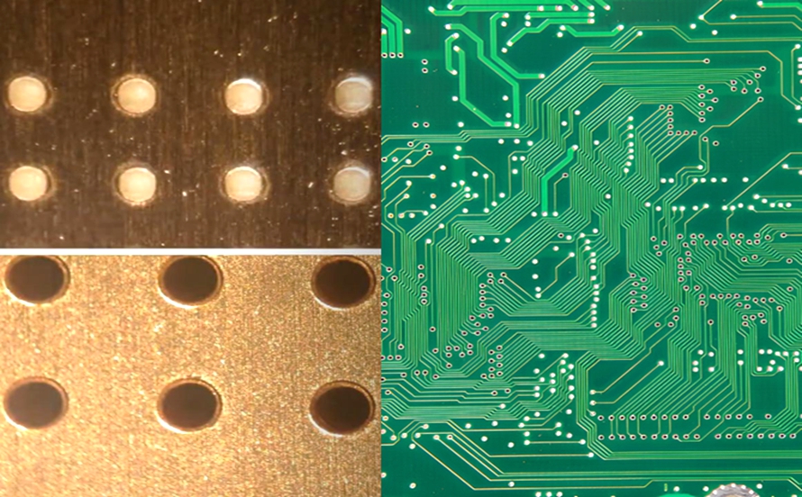
The two broad categories of via filling materials are conductive and non-conductive materials.
The appropriate choice depends on the electrical, thermal, mechanical, and assembly requirements of the PCB.
1. Non-Conductive Via Filling
Non-conductive via filling generally uses an epoxy or other electrically insulating resin to fill the via.
The primary purpose is structural and assembly-related rather than providing an electrical current path through the filling material.
Non-conductive filling can be useful for:
- Via-in-pad structures
- Surface planarization
- Preventing solder wicking
- Supporting fine-pitch component assembly
- Improving mechanical stability
- Filling selected HDI microvias
Vacuum-assisted filling and controlled thermal curing may be used to achieve appropriate filling quality and minimize void formation.
2. Conductive Via Filling
Conductive PCB via filling uses a conductive material, commonly copper-based material or a conductive composite, to provide electrical and/or thermal functionality.
Copper is particularly attractive because of its high electrical and thermal conductivity.
Conductive via filling may be used when the via needs to contribute to:
- Current carrying capacity
- Thermal transfer
- Ground connections
- Power distribution
- Heat dissipation
- Electrical interconnection
In copper-filled structures, the manufacturing process must carefully control plating chemistry, current density, agitation, temperature, and other parameters to achieve uniform deposition.
What Is the PCB Via Filling Process?
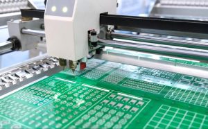
The exact PCB Manufacturing process depends on the PCB structure, via type, filling material, and manufacturer. A typical process may include the following stages.
1. Via Drilling
The process begins by creating the required vias.
Depending on the design, manufacturers may use:
- Mechanical drilling
- Laser drilling
Mechanical drilling is widely used for conventional through-holes, while laser drilling is commonly associated with microvias and high-density structures.
The selected drilling technology depends on the required hole diameter, aspect ratio, layer structure, production volume, and design requirements.
2. Hole Cleaning and Desmear
After drilling, debris and resin smear may remain inside the holes.
The hole walls must therefore be properly prepared before metallization. Chemical or plasma-based processes may be used depending on the manufacturing process.
Effective hole preparation is essential for reliable copper adhesion and subsequent plating.
3. Formation of the Conductive Seed Layer
A conductive layer is established on the hole walls to enable subsequent copper plating.
Electroless copper deposition is commonly used as part of conventional PCB metallization. Other advanced processes may be used for specific manufacturing structures.
The objective is to establish continuous and reliable electrical conductivity throughout the required hole structure.
4. Copper Plating
Copper is deposited onto the prepared hole walls and, depending on the manufacturing design, may also contribute to filling the via.
Electroplating parameters must be carefully controlled to achieve appropriate thickness distribution and filling performance.
Important process variables may include:
- Current density
- Plating chemistry
- Temperature
- Agitation
- Additive concentration
- Plating time
- Panel loading
For advanced filled-via structures, process control is critical because incomplete filling or excessive voiding can negatively affect reliability.
5. Via Filling
The selected filling material is introduced into the via.
For non-conductive filling, specialized epoxy or resin systems may be used. For conductive filling, copper or conductive materials can provide electrical and thermal functionality.
The filling process should minimize:
- Voids
- Cracks
- Delamination
- Incomplete filling
- Surface depressions
6. Curing and Surface Planarization
If a resin-based filling material is used, a controlled curing process is required.
After curing, excess material may be removed through processes such as planarization or surface preparation so that the finished PCB provides a suitable surface for subsequent processing and component assembly.
7. Surface Finishing
Depending on the PCB application, a suitable surface finish may be applied after the relevant surface preparation steps.
Common PCB surface finishes include:
- ENIG
- ENEPIG
- HASL
- OSP
- Immersion tin
- Immersion silver
The appropriate surface finish depends on component pitch, assembly process, environmental requirements, reliability targets, and product specifications.
8. Inspection and Testing
Filled vias should be inspected and tested to verify manufacturing quality.
Potential inspection methods include:
- X-ray inspection
- Cross-sectional analysis
- Microsection analysis
- Dimensional inspection
- Electrical testing
- Reliability testing
For demanding applications, cross-section analysis can provide valuable information about filling quality, voids, cracks, copper thickness, and interfacial conditions.
How Does PCB Via Filling Improve Performance and Reliability?
PCB via filling is not a standard requirement for every PCB. Instead, it is a targeted manufacturing technology used when the design requires specific electrical, thermal, mechanical, or assembly advantages.
1. Supports High-Density PCB Design
Filled vias can be particularly useful in high-density PCB structures.
For example, via-in-pad technology allows vias to be positioned directly within component pads, which can help designers use available board space more efficiently.
This is particularly valuable for:
- Fine-pitch BGAs
- Compact processors
- High-density memory
- Advanced semiconductor packages
- HDI PCB designs
2. Improves Soldering Consistency in Via-in-Pad Designs
One of the most important advantages of via filling is controlling solder movement through vias located in component pads.
If an open via is placed directly in a solder pad, molten solder can flow into the hole during reflow. This may result in inconsistent solder volume at the component interface.
A properly filled and planarized via can reduce solder loss into the hole and provide a more controlled pad surface.
3. Improves Thermal Management
Conductive filled vias can provide an effective thermal path between heat-generating components and copper planes or other thermal structures.
This can be useful for:
- Power electronics
- Processors
- LED systems
- Automotive electronics
- Industrial equipment
- High-power modules
Copper-filled structures can provide a lower thermal resistance path than an air-filled hole, although the actual thermal performance depends on the complete PCB structure and thermal design.
4. Supports Electrical Performance
Via structures can influence high-speed signal behavior through parasitic inductance, capacitance, impedance discontinuities, and return-current paths.
Properly designed and manufactured vias can help maintain controlled electrical characteristics in high-speed designs.
However, via filling itself should not be treated as a universal solution for signal integrity problems. The overall via geometry, anti-pad, reference planes, stub length, stackup, return path, and routing strategy must also be considered during PCB Design.
5. Improves Mechanical Stability
A properly manufactured filled via can provide a more robust structure than an incompletely processed or poorly controlled via.
This can be important in applications exposed to:
- Thermal cycling
- Mechanical stress
- Vibration
- Repeated assembly processes
- High component density
The actual reliability improvement depends on the filling material, copper structure, laminate system, aspect ratio, and manufacturing quality.
PCB Via Filling Design Considerations
Successful PCB Design requires the via structure and manufacturing process to be considered together.
1. Material Compatibility
The filling material must be compatible with the surrounding PCB materials.
Important properties may include:
- Thermal expansion coefficient
- Glass transition behavior
- Moisture absorption
- Adhesion
- Electrical properties
- Thermal conductivity
- Curing characteristics
Material selection should be based on the PCB stackup, operating environment, and reliability requirements.
2. Coefficient of Thermal Expansion
The coefficient of thermal expansion (CTE) is an important consideration.
If the filling material and surrounding materials expand at significantly different rates during thermal cycling, mechanical stress can develop within the via structure.
Over time, excessive stress may contribute to:
- Cracking
- Delamination
- Interfacial separation
- Reliability degradation
Material data sheets and manufacturer process recommendations should therefore be reviewed during material selection.
3. Via Size and Aspect Ratio
Via diameter, depth, aspect ratio, and structure all influence filling difficulty.
As the via becomes deeper relative to its diameter, achieving complete and void-free filling becomes more challenging.
Therefore, via geometry should be established together with the manufacturer’s process capability.
4. Via-in-Pad Requirements
For via-in-pad designs, the filled via generally needs an appropriately planar surface.
Poor planarization can affect:
- Solder paste printing
- Component placement
- Solder joint formation
- BGA assembly reliability
The PCB fabricator and assembly provider should therefore review via-in-pad requirements during the design stage.
5. DFM Considerations
Design for Manufacturing (DFM) is essential when implementing advanced via structures.
The design review should consider:
- Via diameter
- Aspect ratio
- Pad diameter
- Capture pad geometry
- Spacing
- Stackup
- Filling material
- Plating requirements
- Planarity
- Manufacturing tolerances
Early DFM validation can identify manufacturing risks before the design enters fabrication.
Common Problems in PCB Via Filling
Even when the design is correct, poor process control can result in filled-via defects.
Common problems include:
Voids
Voids inside the filling material can reduce mechanical and thermal performance and may become reliability concerns during thermal cycling.
Incomplete Filling
Insufficient filling can leave cavities or depressions that affect surface planarity and assembly performance.
Cracking
Thermal or mechanical stress can cause cracks in the filling material or surrounding copper structure.
Delamination
Poor adhesion or incompatible materials may contribute to separation between the filling material and surrounding PCB structures.
Poor Planarity
An uneven filled-via surface can create problems for solder paste printing and component assembly, particularly for fine-pitch packages.
How to Improve PCB Via Filling Quality
Manufacturers can improve via filling quality by implementing systematic process control.
Important measures include:
- Selecting compatible filling materials.
- Controlling drilling and hole preparation.
- Maintaining stable plating chemistry.
- Controlling current density and plating parameters.
- Optimizing filling pressure or process conditions.
- Controlling curing conditions.
- Maintaining appropriate surface planarity.
- Performing cross-sectional inspection.
- Using X-ray inspection where appropriate.
- Conducting reliability testing for demanding applications.
The exact process window should be established through engineering validation rather than relying on generic parameters.
PCB Via Filling vs. Standard Unfilled Vias
Not every via needs to be filled.
| Feature | Unfilled Via | Filled Via |
|---|---|---|
| Manufacturing complexity | Lower | Higher |
| Cost | Generally lower | Generally higher |
| Surface planarity | Limited | Can be improved |
| Via-in-pad suitability | Limited | Highly suitable when properly processed |
| Thermal functionality | Depends on structure | Can be enhanced with conductive filling |
| High-density applications | Suitable for many designs | Particularly useful for advanced designs |
| Process requirements | Standard | More demanding |
The best choice depends on the electrical, thermal, mechanical, and assembly requirements of the product.
PCB Via Filling and Advanced PCB Manufacturing
As electronic products become smaller and more powerful, advanced PCB Manufacturing technologies are increasingly important.
HDI, microvias, sequential lamination, via-in-pad structures, fine-line routing, and advanced substrate technologies allow engineers to achieve higher component density within smaller footprints.
Via filling is one of the technologies that supports these advanced structures.
However, via filling should not be selected simply because it is technically available. It should be introduced when the product’s performance, assembly, reliability, or space requirements justify the additional manufacturing process.
Choosing a PCB Manufacturer for Filled-Via Applications
When selecting a PCB manufacturing partner for filled-via projects, engineers and purchasing teams should evaluate more than the manufacturer’s basic PCB production capability.
Important questions include:
- Can the manufacturer support microvias and HDI structures?
- What via-filling materials are available?
- Can the manufacturer support via-in-pad?
- What are the available via size and aspect-ratio capabilities?
- How is filling quality inspected?
- Is cross-sectional analysis available?
- Can the manufacturer perform reliability testing?
- Can DFM feedback be provided before fabrication?
- Can PCB fabrication and PCB assembly be integrated?
For complex PCB projects, early communication between the design team and manufacturer can significantly reduce manufacturing risks.
Kingda PCB Manufacturing and Assembly Support
For advanced PCB projects requiring controlled manufacturing and assembly, Kingda provides integrated PCB fabrication and PCBA services.
Kingda’s manufacturing capabilities cover different PCB technologies and production requirements, while its integrated workflow can connect PCB design support, fabrication, component sourcing, SMT assembly, inspection, and testing.
For projects involving HDI structures, high-density layouts, or other demanding PCB technologies, early DFM review can help align the PCB Design with actual manufacturing capabilities.
Conclusion
PCB via filling is an advanced manufacturing technology used to improve specific electrical, thermal, mechanical, and assembly characteristics of a circuit board.
Conductive and non-conductive filling materials serve different purposes. Properly implemented via filling can support via-in-pad designs, improve surface planarity, enhance thermal pathways, support high-density layouts, and contribute to PCB reliability.
However, high-quality via filling depends on much more than the filling material itself. Drilling, hole preparation, metallization, plating, filling, curing, planarization, inspection, and reliability testing must all be carefully controlled.
For engineers developing high-density or high-reliability electronic products, via filling should therefore be considered as part of the complete PCB Design and PCB Manufacturing strategy rather than as an isolated process.
Article Summary
PCB via filling is an important technology for advanced circuit boards, particularly HDI, microvia, and via-in-pad applications. By using conductive or non-conductive filling materials, manufacturers can improve surface planarity, support thermal management, reduce solder wicking, and enable more compact component layouts.
The success of a filled-via design depends on material compatibility, via geometry, plating quality, filling quality, CTE matching, planarization, DFM analysis, and appropriate inspection. Selecting an experienced PCB manufacturing partner is therefore essential for achieving consistent performance and long-term reliability.