PCBA BOM and the Materials Behind a Circuit Board
A bill of materials for an assembled board lists more than the components that will be visible on it. Behind every finished panel there is a second list of materials consumed by the fabricator, and understanding that list is what turns a procurement conversation into an engineering one.
What the PCBA BOM Contains
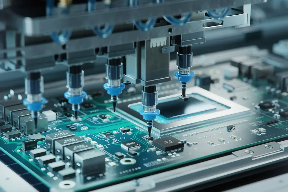
The bill of materials for an assembly covers the printed circuit board itself, the components placed on it, the solder paste and any adhesives, and the consumables that the process needs. Each line is a purchase with its own lead time and its own risk.
The board line is usually the least specific and the most important. Writing only a thickness and a colour leaves the laminate grade, the copper weight and the finish to the supplier, and those three decide most of the electrical and mechanical behaviour.
The Laminate Under Everything
The base material is a resin and glass sheet with copper bonded to one or both faces. The generic name is FR-4, but the name covers a range of resins and glass styles, and the specification that matters is the glass transition temperature, the dielectric constant and the flammability rating.
A higher transition temperature keeps the board stiff and dimensionally stable during assembly, which matters for a thick board or a large panel. The dielectric constant decides the impedance, so it has to be stated wherever a trace is impedance controlled.
Copper Foil
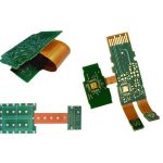
The conductors are formed from the copper that is already on the laminate, and the foil is produced either by rolling or by electrodeposition. Rolled foil is ductile and is used in flexible circuits, while electrodeposited foil is the normal choice for a rigid board.
The weight of the foil sets the finished thickness of the conductor and therefore its current capacity and its resistance. A design that needs more current either increases the weight or the width, and the choice has consequences for the minimum trace and space the fabricator can hold.
Prepreg and the Bond Line
Between the cores there is a sheet of resin impregnated glass that has not yet been cured. It flows under heat and pressure, fills the gaps around the copper and then cross links into a solid, which is what holds the stack together.
Its specification is a thickness and a resin content, and both affect the finished dielectric thickness. When a stackup is changed from one prepreg to another to hit a nominal thickness, the impedance can move with it unless the change is checked.
Dry Film Resist
The pattern is transferred to the copper through a photosensitive film laminated onto the surface. The film is exposed through the artwork and developed, so that the areas that are to remain protected stay while the rest is etched away.
The film exists in a polymerising and a solubilising type, and the choice follows from whether the process images the pattern that is to remain or the pattern that is to be removed. Its resolution sets the finest feature the process can produce.
Solder Mask and Legend
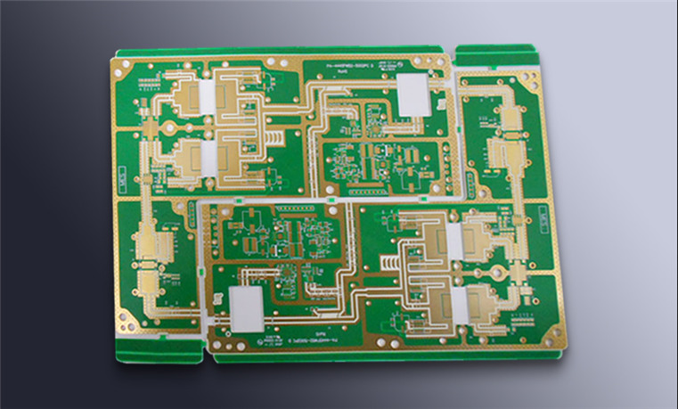
The solder mask is a photoimageable coating printed over the copper and opened only where a joint is required. It is the layer that gives the board its colour and, more importantly, it is what prevents solder from bridging between adjacent pads.
The legend is printed on top of the mask and carries the reference designators and polarity marks. Both layers are defined in the data package, and both are affected by the same ink behaviour during printing and curing.
Artwork and Tooling
The artwork is the master image from which every layer is produced. In a modern shop the design data is converted by a CAM department into the films or the direct imaging files used on the line, and that conversion is where design rule violations are found.
Tooling includes the drill programme, the routing path and any fixtures used for assembly. Each of these is derived from the same data, which is why a mistake in the data package appears in several places at once.
Surface Finish in the BOM
The finish is applied to the exposed copper to keep it solderable. The options range from an organic coating, which is cheap and short lived, to electroless nickel with immersion gold, which stores well and costs more.
The finish belongs in the bill of materials with the storage conditions and the shelf life, because it decides how long the bare board can be kept before assembly. A board that is specified without it will be supplied with whatever the fabricator prefers.
Lead Time and Availability
Every line of the bill of materials carries a lead time, and the longest one sets the schedule. Specialty laminates, fine pitch packages and non standard finishes are the usual candidates, and they should be identified early rather than discovered at the order.
A second source for each critical item is worth the effort before production begins. A single sourced laminate or a single sourced connector is a schedule risk that no amount of production planning can remove.
Keeping the BOM Under Control
The document has to be revision controlled, and the revision used for production has to match the design data. A change of component that is not reflected in the assembly drawing produces a board that is built exactly as the file describes and not at all as the engineer intended.
For the bare board, the fabrication drawing and the stackup are the controlling documents. The materials described there are the ones the copper clad laminate supplier has to meet, and the data package that accompanies them is described in the prototype file checklist.
Process Control and Verification
On a design of this kind, solder mask is the item that decides how the rest of the board is arranged. Running a first article through the same checks as the production panel confirms that the two agree, and that comparison is the cheapest form of process control available at prototype stage. Keeping a sample from the panel turns a dispute into a measurement, because the same coupon can be re-examined by both parties without rebuilding the batch.
Reviewing the design before the data is released is cheaper than correcting it after the panel is in the tank, because every step downstream inherits the decision made at the front end.
Process Control and Verification
On a design of this kind, solder mask is the item that decides how the rest of the board is arranged. Running a first article through the same checks as the production panel confirms that the two agree, and that comparison is the cheapest form of process control available at prototype stage. Keeping a sample from the panel turns a dispute into a measurement, because the same coupon can be re-examined by both parties without rebuilding the batch.
FAQ
Does the bill of materials need to name a laminate brand? Not usually. Specifying the electrical and thermal parameters allows an equivalent to be proposed while keeping the result the same.
Why does prepreg appear in the list? Because it is the bonding layer between cores, and its thickness and resin content affect both the finished board thickness and the impedance.
What is the most common omission? The surface finish and the storage requirement. Both decide whether the boards are still solderable when they reach the assembly line.