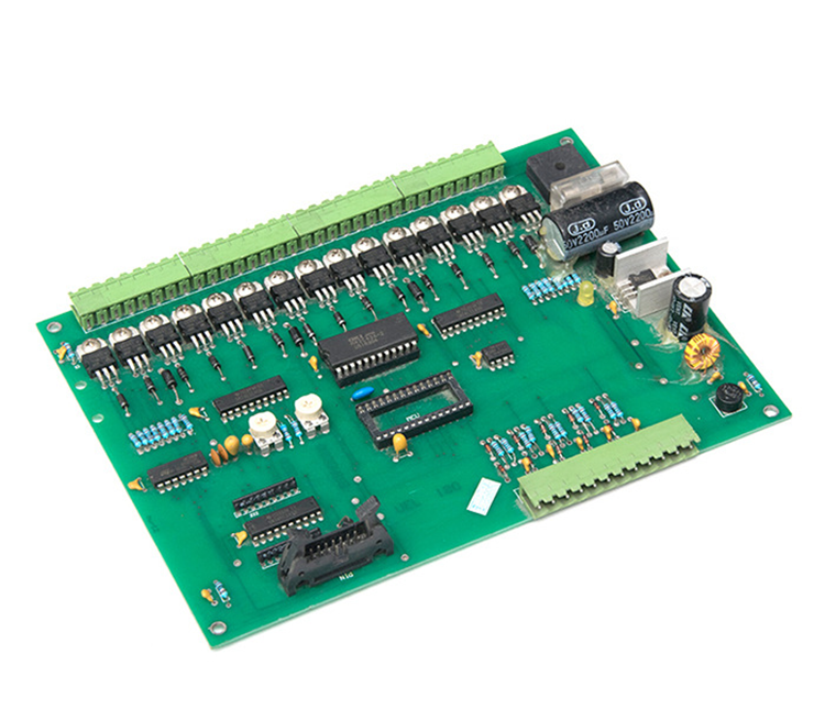
Plating Rectification and Copper Thickness Distribution
Plating rectification is the conversion of alternating current into the direct current that drives copper onto the panel, and the quality of that conversion decides how evenly the metal is deposited. A rectifier that delivers a rough, rippled output produces a deposit that varies in thickness and in grain structure across the same panel.
The plating tank, the chemistry and the racks all have to be right as well, but the electrical supply sets the rate at which the whole system works. Checking it is therefore the first step whenever thickness distribution moves outside its normal band.
What the Rectifier Controls
The rectifier sets the current, and the current divided by the plated area gives the current density that the chemistry responds to. Thickness follows current density and time almost linearly inside the working window, which is why both are controlled rather than one.
It also determines the waveform. A thyristor unit with a coarse firing angle leaves a ripple that the bath sees as a rapidly varying current, while a switch-mode unit with filtering delivers a much smoother output. The rectifier also has to hold its output steady as the load changes, because the resistance of the bath and the racks rises as plating proceeds.
Current Density and Deposition Rate
Copper plating in an acid bath typically runs between 15 and 30 amperes per square decimetre for panel plating. The rate is close to 0.2 micrometres per second at 20 amperes per square decimetre, so a 25 micrometre deposit takes a little over two minutes of plating.
Running above the recommended band increases the deposition rate but reduces throwing power, so the copper builds on the surface faster than it enters the holes. That is how a panel finishes inside the thickness specification and still fails at the barrel. A current density that is set too low produces a fine-grained but slow deposit, and the extended plating time allows more additive to be consumed.
Thickness Distribution Across a Panel
Distribution is the spread of measured thickness across the working area, and it is normally reported as the difference between the highest and lowest reading as a percentage of the average. A well-controlled line holds a spread under 10 percent on a panel with balanced copper.
The pattern of the spread carries information. Copper that is thin at the panel edges points to shielding or to a low current density at the cathode perimeter, while a thin centre points to a resistive bus or a poorly distributed anode load. Throwing power is the ability of the bath to deposit metal inside a hole at the same rate as on the surface, and it falls as current density rises.
Anode Configuration and Shielding
Anodes should face the cathode at a uniform distance, and their area should match the plated area as closely as the rack allows. Where the anodes are shorter than the panel, the current crowds the ends and the deposit is thicker there.
Shielding corrects the geometry that cannot be changed. Insulating shields placed between an anode and the panel edge reduce the current at the perimeter, and their size is found by experiment rather than by calculation, as discussed in the notes on anode area ratio. A panel with unbalanced copper shows a wider spread than a balanced one under the same current, which is why thieving is used on the edges of the rack.
Ripple and Waveform Effects
Ripple appears as a periodic variation superimposed on the direct current, and it affects grain refinement and the distribution of organic additives. A high ripple content produces a deposit that looks dull and measures differently at different points of the same panel.
The ripple should be measured with an oscilloscope at the bus bars rather than at the rectifier terminals. Losses and inductance in the bus run change the waveform that the tank actually sees, and the difference grows with the length of the run. Anode baskets should be topped up so that the anode surface stays below the solution level, because an exposed top section changes the field at the panel edge.
Measurement of Copper Thickness
Thickness is measured on a microsection for the through-hole and on an X-ray fluorescence gauge or an eddy-current instrument for the surface. The three methods do not agree exactly, so the method has to be fixed for a given acceptance criterion.
Measurements should be taken at defined positions rather than wherever the panel happens to be convenient. A map with four corners and a centre is the minimum, and the positions should be marked on the coupon as well as on the drawing. The ripple is normally specified as a percentage of the direct current, and a value under five percent is a common requirement for a plating rectifier.
Corrective Action for Uneven Plating
When the spread grows, the order of investigation is fixed. First the rectifier output and the ripple, then the anode condition and the shield placement, then the bath chemistry and the agitation, and only then the rack loading.
Changing chemistry to fix an electrical problem is the classic error. Adding brightener to a bath that is starving at one corner moves the average thickness without changing the distribution, which leaves the same panel non-conforming at the edge. An eddy-current gauge reads through the solder mask, while X-ray fluorescence needs a defined coating thickness for its calibration, and the two can differ by ten percent.
Acceptance Criteria and Reporting
Acceptance should state the nominal copper thickness, its tolerance, the measurement method and the allowed spread across the panel. It should also state where the through-hole measurement is taken, because the surface and the barrel are separate criteria.
Reporting should include the average, the spread and the position of the extremes. A single average value hides the distribution, and the distribution is what decides whether the smallest annular ring will survive thermal cycling, as discussed in the comparison of panel and pattern plating. A drift in distribution is often the first sign that an anode bag is blocked, because the bag changes the local resistance long before it changes the analysis.
Records and Calibration
Records should carry the rectifier identification, the last calibration date, the ripple measurement, the current and time for each load and the thickness map for the sample panel. gopcb keeps those records with the lot so a drift can be dated.
Rectifier calibration belongs on a schedule that matches its duty. A unit running three shifts drifts faster than one running a single shift, and the calibration certificate alone says nothing about the state of the unit between visits, as noted in the material on rectifier calibration. Any change to the rack, the anode basket or the shield geometry should be followed by a thickness map, since the electrical result follows the mechanical change.
FAQ
What current density is used for copper plating? Between 15 and 30 amperes per square decimetre for most acid copper baths, with the chosen value balancing deposition rate against the throwing power needed for the smallest holes.
Why is the copper thicker at the edges of the panel? The current density is higher at the perimeter, where the surrounding solution offers less resistance, so shielding or a revised anode layout is used to even the field.
How is plating uniformity reported? As the spread between the highest and lowest thickness on the panel, expressed as a percentage of the average, together with the positions at which those values were measured.