Power Plane Design: Current Capacity and Splitting
Power distribution is the part of a layout that is easiest to defer and most expensive to get wrong. It is not a single net with a single rule; it is a set of copper shapes, via arrays and plane boundaries that have to deliver current to many loads without an unacceptable drop, without coupling noise between rails, and without breaking the reference for any signal above them.
This article goes through the factors that decide whether a power plane works: how much current copper and vias can carry, how splits should be shaped, what a voltage drop budget looks like, and how the plane behaves as the second half of the decoupling network.
Current Capacity of Copper
Copper thickness is the first number to establish, because it sets everything else. Standard outer layers are one ounce, roughly thirty-five micrometres, while inner layers are often half an ounce or one ounce. The current a trace can carry at an acceptable temperature rise scales with cross-sectional area, so a half-ounce inner layer needs roughly twice the width of a one-ounce outer layer for the same current.
As a working figure, a one-ounce layer carries about one ampere per twenty mils of width, and a half-ounce layer needs about forty mils for the same current, both assuming a temperature rise of around ten degrees and reasonable airflow. A power plane is simply an extreme case of a wide trace, so the same logic applies: what matters is the narrowest point the current has to pass through, not the area of the plane as a whole.
Via Current Capacity and Layer Changes
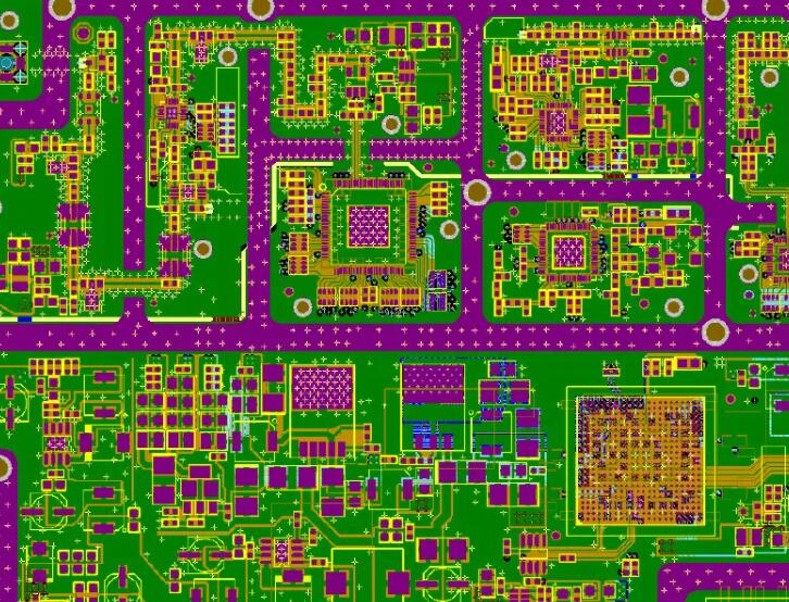
A via is the narrowest point in most power paths. A single ten mil via carries roughly one ampere at a ten degree rise, which means a two ampere rail needs at least two vias, and good practice is to use more than the calculation requires. Vias in a power path also carry heat away from the plane, so a cluster of them under a regulator serves two purposes at once.
The number of vias should be counted twice: once for the current of the rail and once for the switching current of the regulator. A buck converter pulls current in short pulses at the switching frequency, and the via array between the input capacitor, the switch node and the ground return has to handle the peak, not the average. Undersizing that path is a common reason a supply measures well on a bench and fails an emission test.
Plane Splits and the Rules That Keep Them Clean
A power plane carrying several rails has to be split, and the shape of the split matters. Long thin necks and dumbbell shapes are the classic mistakes, because they concentrate current and create inductance exactly where the load needs a low-impedance source. Each rail should be a compact area, and a neck that must exist should be as short and as wide as possible.
The gap between two different rails is also a design parameter. A clearance of roughly twenty mils is a reasonable default, and it can be reduced to about ten mils in a dense area such as under a ball grid array where the copper has to thread between pads. The clearance has to satisfy the voltage difference between the rails as well as the process capability, and the two rails with the largest potential difference are the ones that deserve the most separation.
Voltage Drop and Path Length
Every power path has resistance, and at low voltages the tolerable drop is a small fraction of the rail. A one volt rail with a fifty millivolt budget loses five percent of its headroom, and the copper between the regulator and the load is what consumes it. Keeping the path short is therefore not a layout preference but a numerical requirement.
The trace width and current calculation is the same exercise carried out on a plane shape, and it should be recorded rather than estimated. It runs as follows. The calculation is straightforward: estimate the trace or plane resistance between the regulator output and the farthest load, multiply by the current, and compare the result with the budget. Where the answer is too large, the options are to shorten the path, to widen the copper, to add copper on another layer in parallel, or to move the regulator closer. Adding plane area on a second layer joined by a via array is often the cheapest of the four.
Adjacent Plane Coupling and Overlap
Two planes on adjacent layers form a capacitor, and that is usually useful, but it also means they couple. Where the voltages are similar this is harmless. Where a twelve volt rail runs directly above a one volt rail, the coupling is a noise path, and a switching transient on one appears on the other.
The remedy is not to remove the copper but to change what is opposite it. Placing a ground plane between two dissimilar power planes gives the displacement current a quiet destination and keeps each rail referenced to ground rather than to the other rail. Where a ground layer cannot be inserted, avoiding long parallel overlaps between the two rails reduces the coupled area, and the overlap between rails with the largest voltage difference should be the first to be rearranged.
Signals Crossing a Split
A signal that crosses a plane split has no continuous reference, so its return current has to find a way around the boundary. The detour enlarges the loop, raises the inductance and turns the trace into a radiator. This is the single most common mechanism by which a layout that simulated well produces a board that fails emissions testing.
There are three ways to deal with it. Route the signal so that it does not cross, which is always the best answer; keep the crossing short and place stitching capacitors across the split so the return has a local path; or change the layer so that the signal is referenced to a plane it does not leave. The rules for splitting a power plane describe how to lay the boundaries out so that the crossings are avoided rather than patched.
Decoupling and the Power Plane as a Pair
Above a few megahertz, the plane pair does most of the decoupling work, because the capacitor formed by two large copper areas has a low inductance path to a wide range of points. Below that, the discrete capacitors do the work. The two are not alternatives; they cover different frequency ranges, and the transition between them is where a badly designed power delivery network shows an impedance peak.
The placement of the regulator itself follows the same logic, and the layout and routing rules for a DC-DC converter cover the local loop separately from the plane that distributes its output.
What limits the discrete capacitors is not their value but the inductance of the loop from the capacitor through its vias to the plane and back to the device pin. Two vias per capacitor, placed close together, matter more than an extra hundred nanofarads. Keeping the plane pair thin, or as thin as the stack-up allows, improves the high-frequency behaviour without any change to the components, which makes dielectric thickness a power-integrity decision and not only a signal-integrity one.
FAQ
How wide should a power trace be? Wide enough for the current at the allowed temperature rise, with the narrowest point treated as the limiting case. Compute it from the copper thickness and the current, and remember that a half-ounce inner layer needs about twice the width of a one-ounce outer layer.
Is a plane always better than a thick trace? Not always. A plane is low inductance and easy to use as a reference, but if the current has to funnel through a narrow region the benefit is lost. Local copper shapes sized for the current are often better than a plane that is split into awkward necks.
Do stitching capacitors really fix a crossing? They provide a local return path, which reduces the loop area and the radiation, but they cannot make the reference continuous. Treat them as a mitigation for a crossing that could not be avoided, not as a design technique.