Power Supply Design on a PCB: Requirements and Layout Priorities
Power supply design on a PCB is judged by two things that the schematic cannot express: whether the switching current stays inside the loop that was planned for it, and whether the copper that carries it is wide enough to stay cool. Both are decided by placement and routing, and both are much cheaper to fix before the board is fabricated.
Spacing and Clearance First
Conductor spacing has to satisfy the electrical safety requirement for the working voltage, and it should still be comfortable for production. Where the routing density allows, the spacing on a low-density supply board can be increased at no cost, which improves both the safety margin and the yield. A spacing of roughly eight mil is a common starting point for signal conductors, but supply conductors carrying significant voltage should be placed further apart rather than closer.
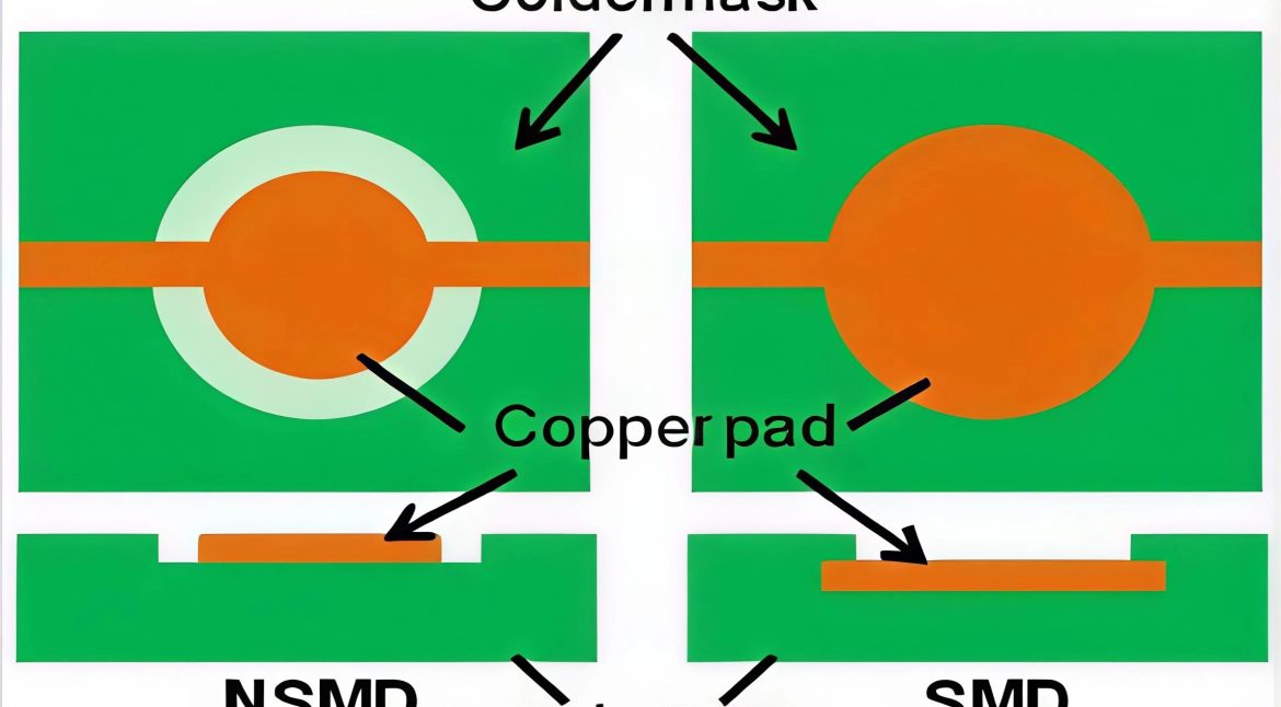
Pad geometry deserves the same care. The edge of a pad should stay more than a millimetre from the board outline, because a pad that is cut by the routing tool is damaged beyond repair. Where a thin trace joins a pad, a teardrop transition improves both the mechanical strength of the joint and the resistance of the pad to lifting during thermal cycling.
The Four Current Loops
Every switching supply contains four current loops: the input source loop, the switch and rectifier commutation loop, the output rectifier loop and the output load loop. The input and output loops carry approximately direct current and are comparatively forgiving. The middle two carry trapezoidal currents with harmonic content well above the switching frequency, peak amplitudes that can reach five times the continuous output current, and transition times near fifty nanoseconds.
Those two loops are the ones that produce electromagnetic interference, and they should be routed before anything else on the board. The filter capacitor, the switch or rectifier and the inductor or transformer that form each loop should be placed adjacent to one another, and their positions adjusted until the path between them is as short as it can be.
Capacitor Terminals Are the Anchors
The input and output filter capacitors, with their decoupling networks, are the reference points of the two quiet loops. Current should flow from the capacitor terminal to the switching stage and back, without sharing a section of copper with any other circuit. Where the connection between the input or output loop and the switching loop cannot be made directly at the capacitor terminal, the alternating energy radiates from the capacitor into the surrounding structure.
That is why capacitor placement is a layout decision rather than a bill-of-materials decision. Two capacitors in parallel, one decoupling ceramic close to the switching device and one bulk part nearby, usually outperform a single larger capacitor placed further away, because the important parameter is the loop the capacitor closes rather than the capacitance value alone. Our bulk capacitor placement notes cover the same point.
Placement Order and Component Grouping
A workable placement order follows the electrical design: place the transformer or inductor, then build the switch current loop around it, then the rectifier loop, then the control circuit that connects to the switching stage, and finally the input and output filter loops. Following that order places the components whose position is fixed by the current paths before the components whose position is flexible.
Within each functional block, place the components around the device that the block serves. Rows of components should be avoided where they lengthen a connection: parallel arrangement looks tidy but a shorter connection between two components is worth more than an orderly appearance. Mechanical parts such as connectors and mounting features come first, since their positions are fixed, and the rest of the layout is arranged around them.

Board Dimensions and Thermal Behaviour
Board size affects both the electrical and the thermal result. A board that is too large lengthens every conductor, which raises the impedance and reduces the immunity of the supply; a board that is too small concentrates heat and brings conductors close enough to couple. A rectangular aspect ratio in the region of three to two or four to three is a reasonable default, and components at the edge should generally be kept a couple of millimetres away from it.
Heat leaves a supply board through the copper and through the interfaces to a heatsink or an enclosure. Thermal relief on the pads that connect to large planes prevents heat from being drawn away during soldering, at the cost of a small increase in impedance, and the trade is worth making wherever hand soldering or rework is expected.
Grounding and Return Paths
Ground is the common return of all four loops, which is why mixing ground types causes instability. In a supply of modest complexity, single-point grounding works: the returns of the input capacitor, the switch, the rectifier and the output capacitor all meet at one place, usually the ground terminal of the filtering capacitor. Where a literal single point is impractical, a compact area of copper shared by several returns gives most of the benefit.
Conductor widths follow the current. Ground should be wider than power, and power wider than signal. A ground trace that is too thin develops a voltage that varies with the switching current, which modulates the reference of the control circuit and appears as jitter. This is where a ground plane earns its place on a supply board. Our switching regulator layout guidance and the thermal management notes cover the details.
Sequencing the Layout Work
A supply layout proceeds in stages, and each stage should be checked before the next begins. The first stage fixes the mechanical constraints: the board outline, the mounting holes, the connector positions and the height limits imposed by the enclosure. The second stage places the magnetics and the power devices, because their positions determine the two noisy current loops. The third stage adds the filter capacitors and the feedback network, and the fourth fills in the control and protection circuitry around them.
Routing then follows the same sequence. The commutation loop is routed first, on the layer directly beneath the device where possible, so that the return current can mirror the outgoing current and cancel much of the field. The gate drive returns and the current sense connections come next, kept short and away from the switch node. Only then are the remaining conductors routed. A decoupling network placed after the high-current paths is far less effective than one placed while the loop geometry is still open to change.
FAQ
Does a supply board need a ground plane? It benefits from one, because a plane keeps the return path directly beneath each conductor and lowers the impedance that the switching current sees. On a two-layer supply board, a ground plane on the reverse side with the components and the supply routing on the front is a common and effective arrangement. Where the board is densely routed and the plane is fragmented, the fragments must be stitched rather than left as isolated pieces of copper.
How much spacing is needed between supply conductors? Enough to withstand the working voltage with margin, plus whatever the fabrication process needs for a reliable yield. The safety requirement sets the floor and the process sets the practical value, and the larger of the two applies. Where the voltage difference is small, the process limit governs; where it is large, the clearance requirement does.
What does gopcb check on a power supply design? We check conductor widths against the current the design carries, the spacing against the working voltage, the clearance from the board edge, the via count on high-current pads and the arrangement of the copper under the switching devices. These are the items that determine whether the supply behaves as designed and whether it can be built repeatedly.