
Preventing Solder Mask Skips and Voids
Solder mask skips are the defects that look trivial and are not. A small area where the ink did not transfer leaves copper exposed, changes the surface the solder sees, and creates a point where contamination can reach the laminate. Because they are small, they are also the defects most likely to pass a visual inspection that is focused on the traces.
What a Skip Looks Like
A skip is an area where the mask is absent, thin or pin-holed. It can appear as a bare copper spot on top of a trace, as a ring around a via where the ink did not release from the screen, or as a scatter of small voids across a plane. Each has a different cause, and they are frequently confused with each other.
Mask voids over a large copper area are usually a printing problem. Skips on individual traces are usually an adhesion or contamination problem. Distinguishing between the two before adjusting anything is what prevents a change that fixes one case and worsens the other.
Screen Printing and Ink Viscosity
Screen printing transfers ink through a mesh onto the board, and the transfer depends on ink viscosity, mesh tension, squeegee pressure and the separation speed between the screen and the panel. An ink that is too viscous will not flow into the openings; one that is too thin will slump after printing and thin out over high features.
Viscosity changes with temperature and with evaporation from the open screen, so a process that is stable in the morning can drift through the shift. Tracking viscosity and keeping the ink within a defined window is a more effective control than adjusting the squeegee when a defect appears.
Adhesion and Surface Preparation
Adhesion between the mask and the copper or laminate depends on the surface it is applied to. Oxide, oil, residue from a previous process step or an insufficiently roughened copper surface all reduce the bond, and a weak bond shows up as a skip that appears after development or after the first thermal cycle rather than at printing.
Surface preparation is therefore part of the mask process, not a separate step. Our notes on PCB etching process control describe how the condition of the copper leaving the etch line affects later processes, and mask adhesion is one of the first things to suffer when that condition varies.
Thickness Variation Across the Panel
Mask thickness is never perfectly uniform. It is thinner over the tops of tall traces and thicker in the gaps between them, and it varies with the copper density across the panel. Where the deposit is thinnest, the film is most likely to break down, which is why skips cluster on the highest features.
Controlling the variation means controlling the copper topography. A layer with less variation in copper height prints more evenly, and a board with heavy copper in one area and fine traces in another will always be harder to mask uniformly than one with a consistent structure.
Cure and the Appearance of Defects
Cure can create its own visible defects. Rapid heating drives solvent out of the film and can produce blisters, particularly where the mask is thick. Under-curing leaves a soft film that marks easily and releases from the surface during handling. Both conditions are visible long before they cause an electrical failure.
The cure profile also affects the apparent severity of a skip. A thin area that looks acceptable after pre-cure may develop a visible void after the final cure as the film shrinks, which is one reason acceptance criteria are applied to the finished board rather than to the printed one.

Where Skips Become Electrical Defects
An exposed copper area is not automatically a defect. It becomes a problem when it allows solder to bridge between two features, when it corrodes in a humid environment, or when it forms a leakage path across a surface that should be insulating. The severity therefore depends on the electrical environment, not on the size of the skip alone.
Our notes on PCB quality inspection describe how acceptance criteria are set against the function of the area rather than against a uniform cosmetic standard, which is the only way to avoid rejecting acceptable boards and accepting defective ones.
Inspection Methods
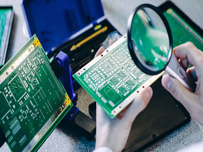
Visual inspection under magnification finds most skips but is slow and depends on the inspector. Automated optical inspection can be programmed to detect missing mask, but the algorithm has to distinguish a real skip from a reflection or a marking dot, and false calls reduce its usefulness.
Our notes on SMT inspection methods describe how board level and assembly level inspection divide the work, and why a mask defect is best identified before assembly rather than inferred from a solder joint afterwards.
Preventing Skips by Design
Some skips are designed in. A mask opening that is smaller than the process can resolve will not print cleanly, and a large copper area with no relief will cause ink to flow and thin out. Keeping features above the process minimum and breaking large planes into a controlled pattern are design decisions that reduce the defect rate.
Where a skip does appear, the fastest route to a fix is usually to compare the defect location with the copper topography. A cluster on the highest features points to thickness, a scatter across a plane points to printing, and an isolated spot on one trace points to contamination.
Corrective Action Sequence
The effective sequence is to classify the defect, check the surface preparation, verify the ink viscosity and printing parameters, and only then consider a change to the cure profile. Changing several variables at once makes the result uninterpretable and often leads to the defect returning after a few weeks.
At gopcb, mask defects are logged with their location and the process conditions of the shift, so that a pattern can be recognised from data rather than reconstructed from memory. That record is what turns a recurring defect into a solved one.
Process Records and Defect Trends
A skip that appears once is an event; a skip that appears at the same location on every panel is a design or artwork problem, and a skip that appears at random intervals across different locations is a process that is drifting. The three patterns are distinguished by the records kept alongside the boards, not by inspecting a single panel more carefully.
Recording the screen, the ink batch, the viscosity reading and the ambient conditions with each lot turns a defect into a data point. After a few months the same record answers questions that would otherwise require a trial: whether a new ink supplier changed the defect rate, or whether a particular product is simply more difficult to print than the others.
The most useful trend to watch is the one that precedes failure. Thin mask and marginal adhesion show up as a rising count of minor skips before they produce a rejected board, and acting on that signal is considerably cheaper than reacting to a field return.
FAQ
Can a solder mask skip be touched up? Small isolated skips can be repaired with a cured ink dot, but the repair has different properties from the original film. Where the area is reliability critical, the board should be treated as non-conforming.
Is a pin hole in the mask a skip? Functionally yes. A pin hole exposes copper and can hold contamination, and it is assessed the same way as a larger opening if it sits on a conductor that must be insulated.
Why do skips appear after cure? Because the film shrinks during cure and a thin area can open into a void. That is why the acceptance check is applied to the finished board rather than to the freshly printed one.