Printed Electronics: Conductive Inks on PCB Substrates
Printed electronics builds circuits by depositing functional materials rather than by etching copper away. A conductive ink is laid down in the required pattern, cured, and the result conducts. The approach removes the etching, plating and lamination steps of conventional fabrication, which makes it attractive for thin, flexible and low cost products. This guide explains how gopcb evaluates printed electronics alongside conventional circuit board processes.
What Printed Electronics Changes
Conventional fabrication starts with a copper clad laminate and removes the unwanted copper. Additive printing starts with a bare substrate and adds only the material that is needed, which reduces chemical consumption and waste. The conductor is thinner than rolled copper, and its conductivity is lower.
That difference defines where the technology fits. Printed conductors suit signal routing, antennas, sensors and low current connections, while power carrying traces and fine pitch component mounting usually remain the domain of etched copper. The two approaches are frequently combined on one substrate.
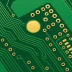
<img src="https://www.gopcba.com/wp-content/uploads/2026/09/271-1.jpg" alt="Conductive ink printed conductors on a flexible substrate” />
Conductive Ink Types
Silver inks offer the highest conductivity and are the most widely used, at a material cost that reflects the metal. Copper inks are cheaper but oxidise readily, so they need a reducing atmosphere or a protective treatment during curing. Carbon based inks are inexpensive and stable but conductive only in a relative sense, which limits them to shielding and sensor electrodes.
Formulations vary further in particle size, solvent system and curing mechanism. A nanoparticle ink sinters at a lower temperature than a flake based ink, which makes it suitable for temperature sensitive substrates, but it costs more and requires tighter storage control to prevent agglomeration.
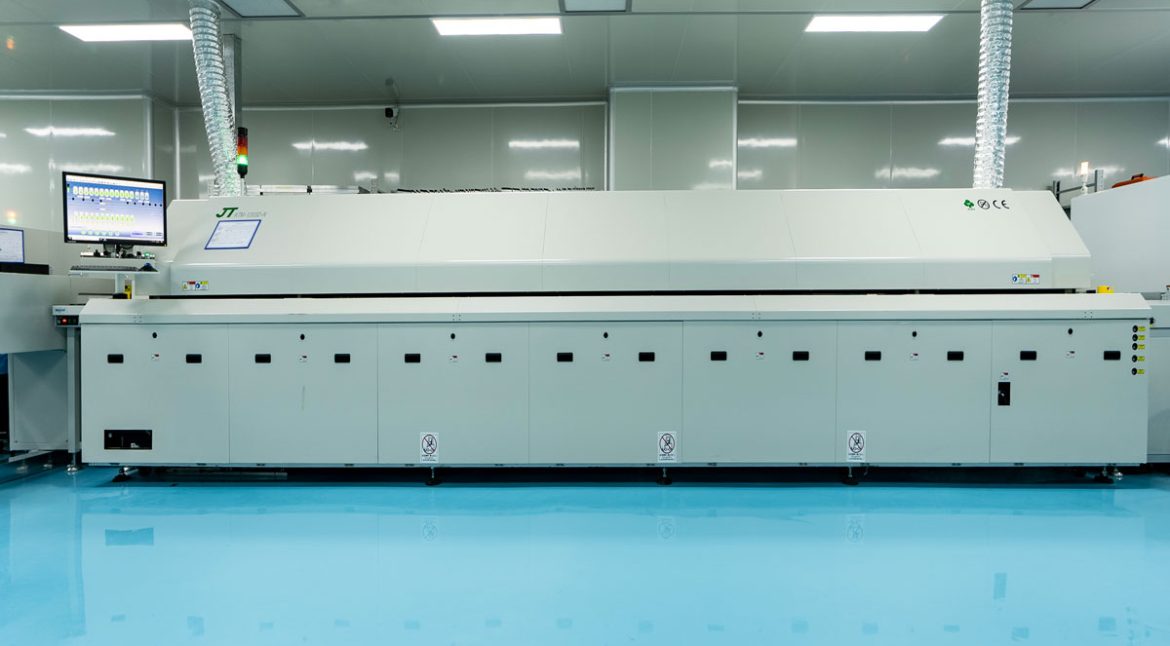
<img src="https://www.gopcba.com/wp-content/uploads/2026/08/Automatic-PCBA-Cleaning.webp" alt="Screen printing of conductive ink for a printed electronics circuit” />
Screen Printing and Other Deposition Methods
Screen printing is the workhorse of printed electronics because it deposits a relatively thick wet layer in a single pass and handles high viscosity inks. Line width is limited by mesh and emulsion quality, and the achievable resolution is coarser than conventional PCB imaging.
Inkjet printing delivers finer features and needs no screen, which suits rapid changes, but deposition is slower and the ink must be formulated for reliable droplet formation. Gravure, flexographic and aerosol jet methods each occupy a different part of the resolution and throughput space, and the choice follows the product rather than the process fashion.
Curing and Sintering
After printing, the ink must be dried and then sintered so that the particles fuse into a continuous conductive film. Drying removes solvent, while sintering forms the metallic connections between particles. Both stages affect conductivity directly, and an incomplete sinter leaves a film that measures high resistance.
Sintering temperature is the constraint that shapes the whole process. High temperature ovens give the best conductivity, but they also limit the substrate to polyimide or glass. Photonic and plasma sintering achieve the same result in milliseconds and allow polyester or paper substrates to be used.
Substrates for Printed Circuits
Substrate choice determines the thermal budget, the mechanical flexibility and the surface smoothness on which the ink is printed. A rough surface interrupts the printed line and raises resistance, so coated papers and planarised films are used where fine features are required.
Flexible substrates dominate the application space because printing suits roll to roll processing. Our notes on bendable circuit materials describe how flexibility and thermal limits interact, and the same reasoning applies when a printed conductor is bent repeatedly.
Resolution and Conductivity Limits
Printed lines are typically tens of micrometres wide at best, and considerably thicker than the copper on a conventional board when measured as a printed film. Conductivity is lower than bulk copper, often by a factor of two to five, so a printed trace of the same width carries less current.
Designers therefore compensate with width rather than with thickness. A printed power line may need to be several millimetres wide to carry a current that a conventional trace would handle in a fraction of the space, which is why printed electronics rarely replaces copper for high current work.
Design Rules for Printed Conductors
Printed conductors follow different rules from etched copper. Minimum line width and spacing are set by the printing method rather than by an etch factor, and the edges of a printed line are less well defined. Design rules should reflect the actual resolution achieved in production, not the best result from a development trial.
Vias and multilayer structures are possible but harder. Printed dielectrics must be pinhole free to insulate crossing conductors, and each additional layer multiplies the yield risk. Keeping a printed design to a single conductive layer with a single crossover layer usually produces the best combination of yield and cost.
Reliability and Environmental Exposure
Printed conductors are more sensitive to humidity than copper traces because the sintered film is porous and the binder absorbs moisture. Resistance rises with moisture uptake, and silver can migrate under bias in the presence of contamination. Encapsulation is therefore normal rather than optional.
Bending fatigue is the other main concern. Repeated flexing cracks the sintered film, and the crack grows until the line opens. Where a printed conductor crosses a flexing region, the design should keep the trace in the neutral axis and avoid sharp direction changes.
Where Printed Electronics Fits
The technology earns its place where a large area must be covered cheaply, where the substrate is flexible or unusual, or where the circuit is simple and the volumes are high. Antennas, touch sensors, heaters, medical electrodes and smart packaging are typical examples.
It also serves prototyping, because a design can be printed and tested without tooling. Where a product needs fine pitch assembly, high current capability or tight impedance control, conventional fabrication remains the correct choice, and the two processes are often used together on the same device rather than in competition.
Process Control and Verification
On a design of this kind, flexible substrate is the item that decides how the rest of the board is arranged. A short note on the drawing about handling, storage or packaging is often worth more than an extra decimal place on a tolerance. Where a value sits close to a process limit, the drawing should say so, since the shop can then open the process window rather than working to a nominal figure that carries no tolerance.
Related reading: our fabrication notes, board quality and design release notes cover the same ground.
Process Control and Verification
On a design of this kind, flexible substrate is the item that decides how the rest of the board is arranged. A short note on the drawing about handling, storage or packaging is often worth more than an extra decimal place on a tolerance. Where a value sits close to a process limit, the drawing should say so, since the shop can then open the process window rather than working to a nominal figure that carries no tolerance.
FAQ
Is printed electronics a replacement for PCB fabrication? No. Printed conductors are limited in resolution, conductivity and current capacity, so they complement rather than replace etched copper. Many products combine printed features for large area functions with a conventional board for the circuit itself.
How conductive is a printed silver ink? Typically two to five times more resistive than bulk copper for the same cross section, depending on the ink and how completely it sinters. Designers compensate by widening traces, which is practical for signal and sensor work but not for high current paths.
Why does printed ink need sintering? Printing deposits discrete particles held together by a binder. Sintering fuses those particles into a continuous metallic network, which is what makes the film conductive. Without an adequate sinter the resistance remains far above the specification.