
RF Power Amplifier Layout Guide
An RF power amplifier converts direct current into radio frequency power, and the layout decides how much of that power reaches the antenna and how much becomes heat. Every millimetre of the ground return and every nanohenry in the matching network changes the result.
What the Layout Has to Achieve
The transistor needs a low impedance path to ground at the source, a matching network that presents the right impedance at the input and the output, and a thermal path that removes the dissipated heat. All three use the same copper.
At radio frequencies a ground connection is not a point but a distributed network. A via of a few tenths of a nanohenry is significant when the impedance being matched is a few ohms, which is why the source is connected with many vias in parallel.
The layout also has to keep the input and the output apart. The gain of a power stage is modest, and a small amount of feedback from the output to the input is enough to make the amplifier oscillate at a frequency where nothing is designed to work.
impedance matching Networks
The transistor is characterised by its source and load impedances for a given output power and linearity, and the matching networks transform the fifty ohm system to those values. The transformation ratio is often large, which means the network has high currents at the device end.
Microstrip lines are the usual implementation above a few hundred megahertz. Their impedance depends on the width, the dielectric thickness and the permittivity, and the layout has to keep the reference plane continuous under them.
At lower frequencies lumped components are used, and their parasitic elements matter. A capacitor that is a good short at a hundred megahertz has significant impedance at a gigahertz, and its self resonance sets the upper limit of its useful range.

grounding and the Reference Plane
grounding in a power amplifier means a low inductance connection to a solid copper plane, and that plane is part of the circuit rather than a return for the supply. The current in it is not small and it flows at the operating frequency.
The source of a field effect transistor should be connected to the plane with a group of vias placed as close to the device as the package allows. A single via a few millimetres away adds enough inductance to reduce the gain and to shift the match.
Slots and splits in the plane under the device are a serious fault, because they force the return current to take a longer path, and the resulting inductance appears in series with the source. A plane that looks continuous on one layer may be broken on an inner one.
thermal via and Heat Removal
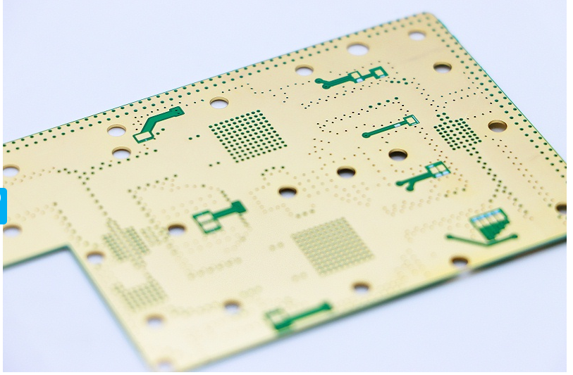
A thermal via array under the device carries the heat to the back of the board, where it can reach a heat sink or a metal chassis. The vias have to be electrically part of the source connection as well, which they usually are in a package with a grounded paddle.
The dice are small and numerous in a good thermal via array, and filled or capped to prevent solder wicking. A large open via under a paddle wicks solder away during reflow and leaves the joint with voids, which raises the thermal resistance.
The copper area on the far side spreads the heat before it reaches the interface material. On a metal backed board the dielectric is thin and the spreading happens in the metal, which is the reason such boards are used at high power.
Decoupling and the Supply Path
The supply current of a power amplifier is modulated at the envelope frequency, and the decoupling network has to supply that current without letting it reach the rest of the system. A combination of a large capacitor and several small ones covers the range.
At radio frequencies the capacitor’s own inductance dominates above its self resonance, so the small capacitors are placed closest to the device and connected with the shortest possible loops. The loop area of the decoupling is as important as the capacitance value.
A bias network often includes an inductor or a quarter wave line that presents a high impedance at the operating frequency while passing the direct current. Its position and its value affect the match as much as the signal path does.
harmonic filter and Output Spectrum
A harmonic filter after the amplifier removes the second and third harmonics that the transistor produces, so that the transmitter meets its spectral mask. It is usually a low pass structure of lumped components or printed elements.
The filter has to present a defined impedance in its pass band and a low one in the stop band, and its insertion loss adds directly to the power that does not reach the antenna. At high power the components have to handle the voltage and the current in the pass band.
The position of the filter matters. Placed after the output match, it works into fifty ohms and is easy to design; placed before, it becomes part of the matching problem. Most designs put it last for that reason.
Stability and Isolation
Feedback from the output to the input is what makes a power amplifier oscillate. The physical separation of the two networks, a ground plane between them and a shielding can where the gain is high are the measures that prevent it.
Stability is verified by driving the amplifier into a mismatched load, because the worst case reflection coefficient is not fifty ohms. A load that reflects most of the power creates a standing wave that can exceed the voltage rating of the device.
An isolator or a circulator at the output protects the device from a bad load, at the cost of insertion loss and size. Where the antenna can be disconnected while the transmitter is running, it is worth the space.
Measurement and Verification
Verify the small signal performance with a network analyser and the large signal performance with a power meter and a spectrum analyser. The small signal match tells nothing about the behaviour at full power, because the device impedance changes with drive.
Measure the temperature of the device and of the board under the thermal vias after a period at full power. A temperature that keeps rising indicates a thermal path that is not conducting as designed, which is often a void in the solder under the paddle.
A layout that works at low power and fails at high power is usually a thermal or a matching problem rather than an assembly fault. The release checks that keep such a board consistent are collected in our PCB design release checklist, and the assembly points are listed in judging PCB quality. The board level measures that contain a radiating structure are described in our guide to EMI suppression design principles.
FAQ
Why do I need so many vias under the device? They connect the source to ground with low inductance. A single via has enough inductance to reduce the gain at the operating frequency.
Should the harmonic filter come before or after the output match? After, where it works into fifty ohms. Placed before, it becomes part of the matching network.
How do I know the amplifier is stable? Test it into a mismatched load, not into fifty ohms. The worst reflection is not the one the design assumes.