Security Surveillance PCB Manufacturing for Reliable Monitoring Systems
Modern security and surveillance systems depend on continuous data collection, stable signal transmission, and reliable electronic control. From security cameras and video surveillance systems to access control equipment, industrial monitoring systems, and intelligent security platforms, the PCB serves as the electrical foundation connecting processors, sensors, communication interfaces, storage devices, power circuits, and other critical components.
A reliable Security Surveillance PCB must do more than simply connect electronic components. It needs to maintain stable electrical performance during continuous operation while handling high-speed image data, power distribution, electromagnetic interference, temperature changes, humidity, vibration, and other environmental conditions.
As surveillance equipment becomes more intelligent and compact, PCB requirements are also becoming more demanding. Higher camera resolutions, AI-based image processing, wireless communication, edge computing, and compact mechanical structures all require more advanced PCB design and manufacturing technologies.
Why PCB Reliability Matters in Security Surveillance Equipment
Security equipment is often expected to operate continuously. A camera installed at a commercial building, transportation facility, industrial site, or outdoor monitoring location may remain powered for long periods with limited opportunities for maintenance.
For this reason, PCB reliability directly affects system availability.
A well-designed Surveillance PCB provides a stable electrical platform for critical functions such as:
- Image and video signal transmission
- Sensor communication
- Processor and memory interconnection
- Power distribution
- Network communication
- Wireless communication
- Storage interfaces
- LED and infrared illumination control
- Alarm and control signal processing
The PCB must maintain electrical and mechanical stability throughout the expected operating environment rather than simply pass initial functional testing.
For applications requiring rapid design verification or specialized security electronics, small-batch PCB prototyping for security surveillance systemscan help manufacturers validate circuit performance before moving into larger production volumes.
Continuous Operation Requires Stable PCB Performance
One of the most important characteristics of a Security Camera PCB is its ability to support continuous operation.
Surveillance equipment may be installed in locations where replacing or repairing hardware is inconvenient or expensive. Outdoor cameras, industrial monitoring systems, traffic surveillance equipment, and remote security devices may need to remain operational for extended periods.
Several PCB characteristics contribute to long-term stability.
Stable Power Distribution
Security cameras and intelligent monitoring devices often integrate processors, image sensors, memory, communication modules, LEDs, motors, and other components on a relatively compact board.
The PCB power distribution network must therefore provide appropriate current capacity and minimize unwanted voltage fluctuations.
Power and ground planes, suitable copper thickness, proper decoupling, and carefully designed return paths can help maintain stable power delivery.
Controlled Thermal Performance
Heat generated by processors, image-processing chips, communication ICs, power regulators, and infrared LEDs can create localized temperature increases.
If heat is not effectively managed, excessive temperature can affect component reliability and electrical performance.
Depending on the design, thermal management may include:
- Large copper areas
- Thermal vias
- Dedicated ground planes
- Heat-spreading structures
- Appropriate component placement
- Thermally optimized PCB stack-ups
The thermal strategy should be developed according to the actual power dissipation and enclosure conditions of the surveillance product.
High-Speed Signal Integrity for Modern Surveillance Systems
Modern surveillance equipment increasingly processes high-resolution video and large amounts of sensor data.
As data rates increase, PCB layout and material selection become more important. Signal integrity problems can result from impedance discontinuities, excessive trace length, poor return paths, crosstalk, electromagnetic interference, or unsuitable dielectric structures.
For high-speed interfaces, a High-Speed PCB should be designed with appropriate attention to:
- Controlled impedance
- Differential-pair routing
- Trace geometry
- Reference planes
- Return-current paths
- Layer stack-up
- Via transitions
- Crosstalk
- Electromagnetic compatibility
For advanced surveillance products using high-speed digital interfaces or RF communication, high-frequency PCB manufacturing provides useful engineering considerations for material selection, lamination, copper characteristics, impedance control, and manufacturing consistency.
Controlled Impedance for High-Speed Interfaces
Certain interfaces used in modern surveillance equipment require controlled impedance to maintain signal integrity.
The actual impedance target depends on the interface specification and system architecture. PCB manufacturers must therefore control dielectric thickness, copper thickness, trace width, spacing, and stack-up parameters according to the approved design.
Small manufacturing variations can affect impedance and signal quality, particularly as signal frequency and data rates increase.
Managing Electromagnetic Interference
Security equipment may operate alongside wireless communication modules, power circuits, motors, switching regulators, and other sources of electromagnetic noise.
PCB design can help manage interference through:
- Appropriate ground-plane design
- Controlled signal routing
- Shorter high-speed paths
- Proper separation of noisy and sensitive circuits
- Differential signaling
- Shielding structures where appropriate
- Optimized layer stack-up
EMI control should be considered during PCB design rather than treated only as a final-stage testing issue.
Environmental Resistance for Indoor and Outdoor Surveillance
Security surveillance equipment may operate in environments ranging from controlled indoor spaces to demanding outdoor installations.
Different applications can expose PCBs to:
- Temperature fluctuations
- High humidity
- Condensation
- Dust
- Vibration
- Mechanical shock
- Corrosive environments
- Long operating periods
A reliable PCB design should therefore consider environmental conditions from the beginning of the project.
Material Selection
Standard FR-4 materials may be appropriate for many surveillance applications, while high-Tg materials or other specialized laminates may be considered when the operating environment or reliability requirements justify them.
Material selection should take into account:
- Operating temperature
- Thermal cycling
- Moisture absorption
- Dielectric performance
- Mechanical stability
- Board thickness
- Manufacturing requirements
The PCB material should be matched to the actual environmental and electrical requirements rather than selected solely according to cost.
Surface Finish and Protection
The PCB surface finish influences solderability, corrosion resistance, contact performance, and assembly reliability.
Depending on the application, manufacturers may select finishes such as ENIG, HASL, OSP, or other appropriate technologies.
For surveillance equipment exposed to humidity, contamination, or harsh environments, additional protection such as conformal coating may also be considered at the assembly level.
PCB Manufacturing Process for Security Equipment
Reliable surveillance electronics require consistent manufacturing across every production stage.
A professional PCB manufacturing process typically involves engineering review, material preparation, circuit formation, lamination, drilling, copper plating, solder mask application, surface finishing, electrical testing, and final inspection.
Each process can influence the final electrical and mechanical performance of the board.
Engineering Review and DFM
Before fabrication, the PCB design should be reviewed for manufacturability.
DFM analysis can identify potential problems related to:
- Trace width and spacing
- Hole sizes
- Via structures
- Copper distribution
- Layer registration
- Board thickness
- Solder mask clearance
- Component assembly requirements
Early engineering review can reduce manufacturing risks and avoid unnecessary design revisions.
Drilling and Plated Through-Holes
Through-holes and vias provide electrical connections between PCB layers.
Their dimensional accuracy and plating quality are particularly important for multilayer surveillance boards where multiple power and signal layers must be interconnected.
Poor hole quality or inadequate plating can affect electrical continuity and long-term reliability.
Electrical Testing
Electrical testing can identify open circuits and short circuits before the finished PCB reaches the assembly stage.
For higher-reliability applications, testing requirements should be defined according to the circuit design, customer specifications, and intended operating environment.
Multilayer PCB Technology for Compact Surveillance Electronics
As surveillance equipment becomes smaller while integrating more functionality, multilayer PCB technology can provide greater routing density within a controlled board area.
A multilayer board can separate power, ground, high-speed signals, low-speed signals, and other circuit functions across different layers.
This can help engineers achieve:
- Higher routing density
- Better power distribution
- Improved signal integrity
- More compact board dimensions
- Better electromagnetic control
- Greater design flexibility
The stack-up must be carefully engineered because dielectric thickness, copper thickness, layer sequence, and reference-plane positioning all influence electrical performance.
For complex surveillance products, the PCB structure should be developed together with the enclosure, component placement, thermal design, and assembly process.
PCB Assembly Quality Also Affects Surveillance Reliability
The bare PCB is only one part of the complete electronic system. Component placement, soldering quality, inspection, and testing also influence the final performance of surveillance equipment.
A complete PCB assembly process may include SMT assembly, through-hole assembly, mixed-technology assembly, inspection, and functional testing depending on the product requirements.
SMT Assembly
Modern security cameras and intelligent monitoring systems often contain compact processors, memory devices, communication ICs, sensors, and power-management components.
SMT assembly enables high-density component placement while supporting compact PCB designs.
Through-Hole Components
Certain connectors, power components, terminals, or mechanically stressed components may require through-hole assembly.
Through-hole technology can provide strong mechanical connections and can be useful for components subjected to mechanical or electrical stress.
Inspection and Testing
Depending on the product, assembly quality can be verified using methods such as:
- AOI
- X-ray inspection
- SPI
- Electrical testing
- Functional testing
- Visual inspection
The appropriate inspection strategy should be determined according to component technology, PCB complexity, and product reliability requirements.
Designing PCBs for Different Surveillance Applications
Not every security device has the same PCB requirements. The board architecture should be matched to the product’s actual function and operating environment.
Security Cameras
Security cameras may require compact PCBs integrating image sensors, processors, memory, Ethernet or wireless interfaces, power management, and infrared illumination.
High-speed signal integrity and thermal management become increasingly important as camera resolution and processing capabilities increase.
Industrial Surveillance
Industrial monitoring systems may require stronger environmental resistance and greater reliability because equipment can operate near machinery, motors, power equipment, or other sources of vibration and electrical interference.
Transportation and Traffic Monitoring
Traffic cameras and transportation monitoring equipment may need to operate outdoors under changing temperatures, humidity, vibration, and continuous power conditions.
The PCB design should therefore consider environmental protection and long-term stability.
Access Control and Security Terminals
Access control equipment may combine RFID, biometric sensors, displays, communication modules, processors, and power circuits on a compact PCB.
High-density multilayer structures can help accommodate these functions within limited enclosure dimensions.
Quality Control for High-Reliability Surveillance PCBs
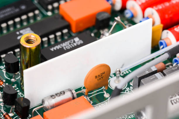
A High-Reliability PCB requires process control rather than relying only on final inspection.
Quality management should cover the complete manufacturing chain, including incoming materials, engineering review, fabrication, assembly, testing, and final inspection.
Important control areas include:
- Material verification
- Lamination control
- Copper thickness
- Hole quality
- Layer registration
- Circuit dimensions
- Surface finish
- Electrical testing
- Assembly inspection
- Production traceability
GOPCBA’s manufacturing capabilities cover multilayer, HDI, high-frequency, high-speed, heavy copper, rigid-flex, and other advanced PCB technologies, allowing PCB construction to be matched to different electronic applications. PCB capabilities can be evaluated according to layer count, material, copper weight, board thickness, trace geometry, and other technical requirements.
From Prototype Validation to Production
Surveillance products frequently undergo several design revisions before entering stable production.
A practical development process can include:
- PCB design and engineering review
- Prototype fabrication
- Prototype assembly
- Electrical and functional testing
- Design optimization
- DFM/DFA review
- Pilot production
- Volume manufacturing
- Final quality inspection
This approach allows engineers to identify signal integrity, thermal, mechanical, and assembly issues before production quantities increase.
For security equipment manufacturers, the ability to transition from prototype to production with consistent manufacturing controls can reduce development risk and improve product launch efficiency.
Conclusion
The PCB is a fundamental part of modern security and surveillance equipment. It provides the electrical infrastructure required for image processing, data communication, power distribution, sensor integration, and system control.
A reliable Security Surveillance PCB must support continuous operation while maintaining signal integrity, thermal stability, environmental resistance, and consistent manufacturing quality.
As surveillance systems move toward higher resolution, AI-assisted processing, faster communication, smaller form factors, and greater functional integration, PCB requirements will continue to evolve.
The most reliable approach is to evaluate PCB material selection, layer structure, signal integrity, thermal management, manufacturing feasibility, assembly requirements, and testing as one integrated engineering system.
With appropriate design and manufacturing controls, Surveillance PCB technology can provide the stable electrical foundation required for security cameras, industrial monitoring systems, access control equipment, intelligent surveillance platforms, and other critical security applications.