In High-Speed PCB design, differences in trace length can create propagation-delay mismatches that affect signal timing, especially when multiple signals must arrive at their destinations within a narrow timing window. Serpentine Routing is commonly used to compensate for small length differences and achieve more accurate Length Matching between related signals.
However, serpentine routing should not be treated simply as a way to “make traces longer.” Poorly designed serpentine traces can introduce additional coupling, Crosstalk, impedance discontinuities, and signal-quality degradation. Therefore, the purpose and geometry of serpentine routing should be carefully evaluated during PCB Routing.
What Is Serpentine Routing?
Serpentine routing is a PCB trace pattern in which a signal trace is intentionally routed back and forth to increase its physical length within a limited PCB area.
It is most commonly used when several signals belong to the same timing group and their propagation delays need to be closely matched. Typical applications include:
- High-speed parallel data buses
- Differential signal groups
- Memory interfaces
- Clock and strobe signals
- High-speed processor interfaces
- FPGA and high-speed digital interconnects
The primary purpose of serpentine routing is Length Matching, not filtering or intentionally creating an inductor.
Why Trace Length Matching Matters
Every PCB trace introduces a finite Propagation Delay. When a high-speed signal travels through a longer trace, it generally takes more time to reach the receiver than a signal traveling through a shorter trace.
For a group of related signals, excessive delay differences can cause timing uncertainty. If the receiver samples the signals before all relevant bits have settled, setup and hold margins may be reduced, potentially resulting in data errors.
For this reason, high-speed interfaces often specify a maximum allowable length mismatch or skew between related signals.
The required tolerance depends on the interface, signal rise time, operating frequency, stackup, dielectric material, trace geometry, and system timing budget. Therefore, a universal rule such as “the delay difference must always be less than one-quarter of the clock period” should not be applied to every PCB design.
Instead, designers should determine the allowable skew from the actual interface specification and timing budget.
The Relationship Between Trace Length and Propagation Delay
Propagation delay is influenced by the electrical characteristics of the transmission line, particularly the effective dielectric constant of the surrounding PCB material and the trace geometry.
A simplified relationship can be expressed as:
Propagation Delay ≈ Trace Length × Delay per Unit Length
The delay per unit length is affected by factors such as:
- Dielectric constant and effective permittivity
- Dielectric thickness
- Trace width
- Copper thickness
- Transmission-line structure
- Reference-plane configuration
- Material construction
Consequently, simply matching the physical length of two traces does not always guarantee perfectly matched electrical delay.
This becomes increasingly important in High-Speed PCB applications, where manufacturing tolerances and material variations can consume part of the available timing margin.
Serpentine Routing for High-Speed Signals
When a trace requires additional length, a serpentine pattern can provide the required compensation without significantly increasing the overall routing area.
For example, if one data line is shorter than the other signals in the same timing group, the designer may introduce a controlled serpentine section to increase its effective path length.
However, the added routing should be as electrically clean as possible.
A well-designed serpentine trace should consider:
- Required additional length
- Trace width
- Spacing between adjacent segments
- Reference-plane continuity
- Number of bends
- Bend geometry
- Signal rise/fall time
- Controlled Impedance requirements
- Potential coupling to neighboring traces
The goal is to achieve the required delay compensation without introducing unnecessary discontinuities.
Serpentine Routing and Crosstalk
One of the most important disadvantages of serpentine routing is increased coupling between adjacent sections of the same trace.
When parallel segments are routed close together, electric and magnetic fields can couple from one segment to another. This may produce additional Crosstalk and can modify the waveform seen by the receiver.
The problem becomes more significant when:
- Signal rise time is very fast
- Parallel sections are long
- Spacing between segments is small
- The trace is routed over an uninterrupted reference plane
- Multiple high-speed signals are routed closely together
Therefore, serpentine routing should not simply maximize the amount of trace that can fit into a given area.
How Much Spacing Should Be Used?
The spacing between adjacent serpentine segments is an important design parameter.
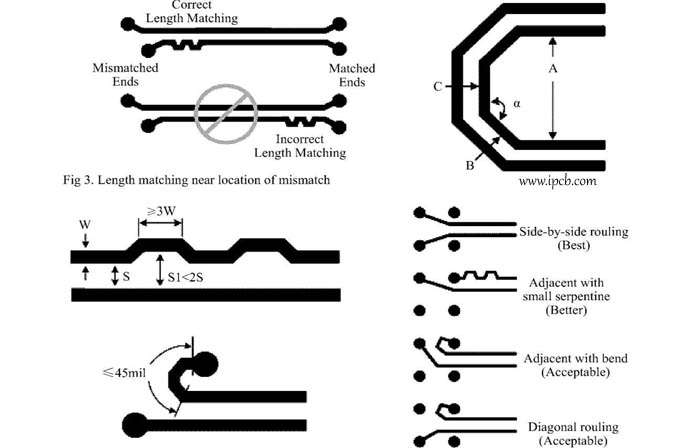
A common practical approach is to keep adjacent segments sufficiently separated to reduce coupling. A spacing of approximately 3W or more, where W is the trace width, is often used as a conservative starting point for general high-speed routing. However, this is not a universal requirement.
The appropriate spacing depends on:
- Signal rise time
- Trace geometry
- Layer structure
- Dielectric thickness
- Reference-plane distance
- Required skew tolerance
- Acceptable crosstalk level
For particularly fast interfaces, electromagnetic simulation or field-solver analysis can provide a more accurate evaluation than relying on a simple spacing rule.
Why Excessive Serpentine Routing Can Be Harmful
Adding unnecessary meanders can make a PCB more difficult to route and may reduce signal quality.
A long serpentine section can create:
- Additional coupling
- Increased parasitic capacitance
- Increased parasitic inductance
- Local impedance variation
- Reflections
- Additional propagation delay
- Greater sensitivity to manufacturing tolerances
The electrical length of the trace also matters more than its appearance. A compact-looking serpentine structure may still create substantial coupling if adjacent segments run parallel for a long distance.
Therefore, designers should use the minimum additional routing length required to satisfy the timing constraint.
Serpentine Routing Is Not Normally a Filter Inductor
Some older PCB design discussions describe serpentine traces as “filter inductors.” This description can be misleading in modern high-speed digital design.
A PCB trace naturally has distributed resistance, inductance, and capacitance. A serpentine structure can increase these parasitic effects, but that does not mean it should automatically be considered an intentional LC filter.
If a circuit requires filtering, impedance matching, or RF inductance, the component and transmission-line structure should be intentionally designed for that function.
For ordinary high-speed digital buses, the primary purpose of serpentine routing is Length Matching and timing compensation.
Serpentine Routing for Clock and Data Signals
Clock signals deserve particular attention because they establish the timing reference for related data signals.
However, this does not mean that every clock trace should automatically be routed with a serpentine pattern.
For a synchronous interface, designers should evaluate the complete timing relationship between:
- Clock
- Data
- Strobe
- Control signals
- Receiver setup time
- Receiver hold time
- Driver and receiver characteristics
In many interfaces, matching data-to-data length is only one part of the timing problem. Clock-to-data skew and package delay may also contribute significantly to the overall timing budget.
Therefore, PCB Routing should be based on the interface’s actual timing requirements rather than a simple “equal length everywhere” rule.
Example: High-Speed Bus Length Matching
Consider a high-speed digital interface with multiple related data lines. If one trace is substantially shorter than the others, its signal may arrive earlier at the receiver.
Instead of unnecessarily rerouting the entire bus, the designer may add a controlled serpentine section to the shorter trace.
The objective is not necessarily to make every trace exactly identical in physical length. The better approach is to keep the electrical delay difference within the tolerance required by the interface.
This distinction is especially important for advanced High-Speed PCB designs.
Differential Pair Serpentine Routing
Differential pairs require additional care.
The two traces in a differential pair should generally maintain consistent:
- Trace width
- Pair spacing
- Reference-plane relationship
- Electrical length
- Coupling environment
If additional length is required, the serpentine section should preserve the differential-pair geometry as much as possible.
An improperly designed meander can introduce common-mode conversion, local impedance variation, and additional coupling between the two conductors.
Therefore, differential-pair length matching should be considered together with differential impedance and pair symmetry rather than as an isolated physical-length requirement.
Practical Guidelines for Serpentine Routing
The following guidelines can help improve serpentine routing in high-speed PCB designs:
1. Use serpentine routing only when necessary.
Do not add meanders simply because equal trace lengths appear aesthetically desirable.
2. Match electrical delay, not just physical length.
Consider dielectric properties, trace geometry, and stackup when tight timing margins are involved.
3. Maintain sufficient spacing.
Increase the spacing between adjacent serpentine segments to reduce coupling and Crosstalk.
4. Minimize long parallel sections.
Long, closely spaced parallel sections increase capacitive and inductive coupling.
5. Maintain the reference plane.
Avoid routing serpentine sections across plane splits, voids, or other discontinuities.
6. Avoid excessive bends.
Use smooth or controlled-angle bends where appropriate, particularly for very high-speed signals.
7. Preserve controlled impedance.
The serpentine geometry should remain compatible with the intended Controlled Impedance structure.
8. Consider the signal rise time.
A signal with a very fast edge can behave as a high-speed transmission-line signal even when its nominal clock frequency is relatively low.
9. Verify critical designs through simulation.
For demanding interfaces, signal-integrity simulation can evaluate the effects of coupling, reflections, impedance variation, and timing skew.
Common Mistakes in Serpentine Routing
Several common design practices can reduce the effectiveness of length matching.
Making Every Trace Exactly the Same Length
Perfect physical equality is not always necessary. Excessive meandering can actually introduce more coupling and signal-integrity problems than the original length mismatch.
Placing Serpentine Segments Too Close Together
Tight spacing increases coupling between adjacent sections and can distort the waveform.
Ignoring Reference-Plane Continuity
A trace routed over a discontinuous reference plane may experience a changed return-current path and increased electromagnetic interference.
Matching Length Without Checking Timing
The required matching tolerance should come from the interface timing budget. A fixed length-matching number is not appropriate for every application.
Using Serpentine Routing as an RF Filter
Serpentine traces should not be treated as general-purpose filtering components. If filtering is required, the circuit should be designed specifically for that purpose.
The Role of Manufacturing in Length Matching
For high-precision PCB Manufacturing, the final electrical characteristics of a trace depend not only on the CAD layout but also on fabrication tolerances.
Parameters such as trace width, copper thickness, dielectric thickness, layer registration, and material properties can vary within manufacturing tolerances.
These variations can influence:
- Characteristic impedance
- Propagation delay
- Differential skew
- Coupling
- Signal attenuation
For critical high-speed interfaces, designers should therefore include realistic manufacturing tolerances when establishing length-matching requirements.
Kingda’s Approach to High-Speed PCB Routing
At Kingda, high-speed PCB fabrication is evaluated from both design and manufacturing perspectives. For projects requiring tight timing control, our engineering team can consider stackup structure, controlled impedance, trace geometry, material selection, copper thickness, layer registration, and manufacturing tolerances.
Instead of relying only on nominal trace lengths, the design should be evaluated against the actual electrical and manufacturing requirements of the application.
This approach helps reduce unnecessary serpentine routing while supporting stable signal integrity and reliable high-speed performance.
Conclusion
Serpentine Routing is an important technique for achieving Length Matching in high-speed PCB design. Its primary purpose is to compensate for controlled differences in signal path length and reduce propagation-delay mismatch between related signals.
However, serpentine routing is not simply a method for making traces longer. Excessive or tightly spaced meanders can increase coupling, Crosstalk, parasitic capacitance, parasitic inductance, and impedance variation.
For modern High-Speed PCB designs, effective PCB Routing should therefore balance timing requirements, signal integrity, controlled impedance, reference-plane continuity, and manufacturing tolerances.
By using serpentine routing only where necessary and designing its geometry carefully, engineers can achieve the required timing performance without introducing unnecessary signal-integrity risks.