Smart Glasses PCB Cost Guide: Materials, Design and Price Factors
Smart glasses have become one of the most innovative product categories in consumer electronics, and at the center of every pair is a carefully engineered smart glasses PCB. This small board connects sensors, processors, wireless modules, and display drivers inside a frame that must remain light, thin, and comfortable. For OEM brands and startups alike, understanding the cost structure of smart glasses PCB manufacturing is essential for budgeting and for keeping the final product competitive. This guide breaks down the materials, design choices, price ranges, and cost-saving strategies that define smart glasses PCB production.
What Is a Smart Glasses PCB?
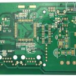
A smart glasses PCB is the electronic control board inside wearable eyewear. It connects and controls several subsystems, including motion and gesture sensors, Bluetooth and Wi-Fi wireless modules, battery management circuits, and display and audio synchronization electronics. Because the glasses frame is curved and thin, smart glasses commonly use flexible PCB or rigid-flex PCB designs that bend to fit the structure. These boards typically run six to ten layers and require precision drilling and fine-pitch placement, which raises manufacturing complexity compared with standard rigid boards.

Materials and Design Cost Drivers
The largest share of smart glasses PCB cost comes from material selection and circuit design complexity. FR4 rigid boards are the most economical option, typically costing less per board. Polyimide flexible material costs more because lamination and high-temperature processing are more demanding. Rogers or mixed high-frequency laminates add further cost and are used when the antenna or wireless performance demands it. For most smart glasses projects, a mid-range rigid-flex combination offers the best balance of flexibility, reliability, and cost, especially when the layout is optimized early.
The design phase has a direct effect on price. A layout with excessive layers, long routing, or unnecessary microvias inflates both fabrication and yield risk. Having the PCB design and layout team review the board before release helps reduce layer count and routing length, which typically trims a meaningful share of the prototype cost.
Key Factors That Affect Smart Glasses PCB Price
Several variables determine the final price of a smart glasses PCB. Material type is the first factor, followed by the number of layers and the board size. The use of HDI technology, which adds microvias and dense interconnect, increases cost but enables the miniaturization that smart glasses demand. SMT assembly of miniature components raises difficulty and therefore price, and the precision of electrical and functional testing affects both yield and unit cost. All of these factors interact, so the cheapest quotation is rarely the one that meets your yield and reliability targets.
Smart Glasses PCB Price Ranges in 2025
Prices differ by production stage. Engineering samples for research and functional validation typically range higher per board because of tooling, low volume, and manual setup. Small-batch production for market testing or pilot runs costs less per unit, and volume production brings the unit price down substantially as setup and material costs are amortized. Flexible board variants usually cost more than rigid designs of similar complexity because of material and process overhead. In practice, total per-board cost can range from a few dollars in high volume to tens of dollars for small engineering quantities, with the exact figure set by layer count, material, and testing requirements.

Regional Cost Comparison
Manufacturing location changes the economics significantly. China remains the most cost-effective region for smart glasses PCBs thanks to a complete supply chain, experienced operators, and highly automated lines. US and European production offers shorter logistics in some cases but carries higher labor and equipment costs, and European sourcing often has longer lead times for this type of board. Even after international shipping and duties, sourcing from a capable Chinese supplier can reduce total board cost substantially for volume programs.
How a Full-Service Manufacturer Reduces Cost
The most effective way to control smart glasses PCB cost is to consolidate design support, fabrication, and assembly under one supplier. An in-house SMT line removes outsourced assembly fees, centralized material purchasing reduces raw material expense, and free design-for-manufacturing review catches layout problems before tooling is committed. A flexible MOQ that supports small prototype orders lets startups validate the design without paying for volume. One partner also removes the logistics and management overhead of coordinating several vendors.
For wearable programs that mix rigid sections with flexible interconnects, working with a team that runs flex PCB assembly in-house keeps bend areas reliable and avoids handoff damage between separate fabricators and assemblers.
Additional Costs OEMs Should Plan For
Beyond board fabrication, smart glasses brands should budget for design revisions and repeated prototyping, key component procurement such as processors, sensors, and wireless chips, and functional testing and certification such as CE and RoHS. Component sourcing deserves special attention because wearable supply chains shift quickly. A supplier with strong component procurement can lock in availability and pricing for long-lead parts while the board design is still being finalized.
Common Challenges in Smart Glasses PCB Design
Smart glasses boards push every dimension to its limit, which creates a predictable set of engineering challenges. Antenna placement is the most visible one: Bluetooth and Wi-Fi performance collapse when the antenna sits next to a ground pour or a metal hinge, so the layout must reserve a clean keep-out zone. Battery capacity is limited by frame size, forcing the power management circuit to run efficiently across wide current swings. Display routing must isolate high-speed video signals from sensor lines to avoid image noise and false gestures. Bending zones in rigid-flex designs need teardrop pads and staggered transitions so repeated flexing does not crack the copper. Finally, component height must be controlled strictly because the lens assembly and hinge mechanics leave almost no vertical clearance.
Most of these problems are solved in the design review rather than on the production line. A manufacturer that reviews the stack-up, flex bend radius, and antenna keep-out before tooling will save you both time and redesign cost.
Practical Tips to Lower Smart Glasses PCB Assembly Cost
Start by optimizing the circuit layout to reduce layers and routing length. Use economical FR4 material during the prototyping stage when full flexible performance is not yet being validated. Choose a supplier that provides fabrication and assembly together, and plan batch sizes ahead of time to qualify for lower unit pricing. Finally, verify that testing is aligned with your product risk: basic electrical testing should always be included, while advanced functional testing can be added where field reliability demands it.
Conclusion
Smart glasses PCB cost is shaped by material selection, design complexity, production volume, and the capabilities of your manufacturing partner. By optimizing the layout early, using the right material for each development stage, and consolidating fabrication and assembly with one experienced supplier, you can control cost without compromising the thin, flexible, reliable boards that wearable products require.
Frequently Asked Questions
Q1. What is the minimum order quantity for smart glasses PCB prototypes? Many manufacturers accept orders as small as five to ten boards for engineering samples, which lets startups validate designs without committing to volume.
Q2. How long does smart glasses PCB production take? Typical lead times range from seven to fifteen working days depending on layer count, material, and testing requirements, with faster options available for simple designs.
Q3. Can suppliers build flexible and rigid-flex boards for wearables? Yes, rigid-flex and flexible PCB production is standard for wearable devices. Confirm that the supplier controls both lamination quality and PCBA testing so the final assembly is verified as a complete unit.