SMD Package Classification: From Chip Components to BGA
Surface mount technology reshaped electronics by shrinking components to a fraction of their through-hole ancestors, and the packages that resulted are numerous enough to confuse anyone meeting them for the first time. Understanding how they are classified makes datasheets, assembly quotations and layout libraries far easier to read, because the package name tells you how the part is placed and how the joint is formed.
What Surface Mount Technology Changed
Surface mount technology is the dominant assembly method in the industry. Components are placed on pads on the board surface and joined by reflowing solder paste, rather than being inserted through drilled holes and soldered from beneath. The gain is density: components became a fraction of their former size, which allowed products to become smaller, lighter and cheaper to build at volume.
The terminology follows the technique. A surface mount device is usually abbreviated SMD, and the same parts are also called SMC, or chip components, depending on the convention. The process of assembling them is SMT, and the machines that do the work are SMT equipment. The distinction between the part and the process matters when specifying anything.
SMD Versus SMC: Terminology and Scope
The two abbreviations overlap in practice. SMD generally refers to the device itself, while SMC is often used for the simpler chip-style parts with two terminals. In common usage the terms are interchangeable, and both cover the entire family from a tiny resistor to a complex processor package.
What unites them is the attachment method rather than the form. Every one of these parts is designed so that its electrical connection is made on the same surface on which it sits. That constraint drives the design of the package: terminations must be accessible from below or from the side, and the body must be stable enough to be picked, placed and reflowed without damage.
Two-Terminal Chip Components
The simplest family consists of two-terminal parts. Resistors, capacitors, inductors and diodes in chip form dominate the component count on most boards, and their package codes describe physical size rather than electrical value. They are supplied on tape and reel, fed by the placement machine, and positioned by vision before being released onto the paste.
Because they are so numerous, they drive the economics of assembly. A smaller case size permits higher density but demands tighter paste printing, better placement accuracy and cleaner stencils. Choosing the smallest available part without considering the assembly process is one of the most common ways to create yield problems on an otherwise straightforward design.
Leaded and Leadless Integrated Circuit Packages
Integrated circuits then divide into families by how they present their connections. Small outline packages have leads on two sides and remain common for modest pin counts. Quad flat packages, usually written QFP, carry leads on all four sides and support much higher pin counts, with fine pitch versions reaching lead spacings that challenge both printing and placement.

Leadless variants replace the leads with flat pads around the body. They save space and reduce lead inductance, which helps at high frequency, but they offer less compliance between the package and the board. That compliance is what absorbs thermal expansion mismatch, so a leadless part demands a well matched footprint and a controlled reflow profile. Footprint geometry for these packages is discussed in PCB pad design standards.
Area Array Packages: BGA, CSP and Flip Chip
Area array packages move the connections underneath the body. A ball grid array uses a grid of solder balls across the underside, which allows very high pin counts without fine peripheral pitch. A chip scale package applies the same idea at a size only slightly larger than the die itself, and flip chip goes further by connecting the die directly through bumps rather than wire bonds.
These packages are electrically excellent, because short interconnections reduce inductance, and they free the board surface around the part for routing. Their drawback is inspection: the joints are hidden, so assembly verification moves from optical inspection to X-ray, and rework becomes a specialist operation. Multi-chip modules extend the family by combining several dies in one package, which is described in IC package substrate.
Functional Classification: Interconnect, Active, Passive and Odd-Form
A second way to classify these parts is by function. Interconnect components provide mechanical and electrical connection or disconnection, and consist of a plug and a receptacle that join cables, racks, chassis or one board to another. Even these must attach to the board by a surface mount termination to belong in this group.
Active components control voltage and current within a circuit, producing gain or switching, which means they respond to the applied signal and change their own characteristics accordingly. Passive components do not change their behaviour when a signal is applied and simply provide a predictable, repeatable response. Odd-form components are the exception: their geometry is unusual, often because the package was designed for function rather than for placement, so they must be inserted by hand. Transformers, hybrid assemblies, fans and mechanical switch blocks are typical examples.
Designing and Assembling Mixed Package Types
Real boards rarely use one family. A typical design mixes chip components, fine pitch peripherals, one or two area array devices and the occasional odd-form part, and each contributes a different constraint to the assembly process. The process window has to accommodate all of them at once, which usually means the tightest package sets the paste volume and the profile.
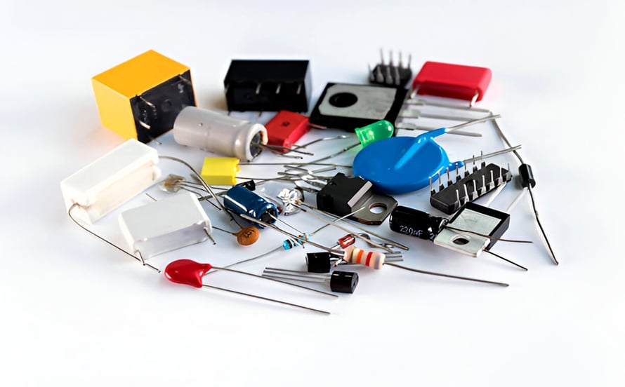
Odd-form parts deserve early attention, because they are placed by hand and often need to be soldered separately. Their position affects the order of assembly and may force additional handling or a second reflow. Deciding where they go during layout, rather than discovering them when the line is being programmed, keeps the process simple. Process capability for these mixed assemblies is covered in SMT process window capability and the inspection sequence in SMT inspection methods.
Reading a Package Code
Package codes are compact, but they are systematic once the pattern is recognised. The letters describe the shape and the arrangement of the terminations: small outline, quad flat, ball grid, chip scale. Numbers appended to the code usually give the pin count, and a suffix indicates the pitch, the body size or the thermal variant.
A few conventions are worth memorising. Thin and low profile prefixes indicate reduced body height, which matters where clearance above the board is limited. Exposed pad suffixes mean the package carries a thermal pad underneath, and that pad must be soldered to a copper area with vias if the design is to dissipate the heat the package was chosen for. Ball pitch, rather than ball count, is what usually decides whether a ball grid array can be routed on a given layer count.
The practical consequence is that a package code should never be treated as a procurement detail alone. It determines the footprint, the stencil aperture, the placement accuracy required, the inspection method and, in the case of a thermal pad, part of the power design. Recording all of that in the component library at the time the part is selected is far cheaper than reconstructing it later from a datasheet.
FAQ
What is the difference between SMD and SMT? SMD refers to the component, while SMT refers to the technology and process used to assemble it. In practice the two are often used loosely, but the distinction is useful when writing specifications.
Why do ball grid array packages need X-ray inspection? Because the solder joints sit underneath the package body, where no camera can see them. X-ray reveals bridging, voiding and joint size, which optical inspection cannot.
What makes a component odd-form? An unusual or non-standard body shape that cannot be handled by a placement nozzle. These parts are placed by hand, and their position should be planned during layout rather than discovered during assembly.