




SMT Component Selection Guide for PCB Assembly
SMT component selection is one of the first and most important steps in PCB design. The component package determines how the part is placed, soldered, inspected, and tested. A well-chosen package saves PCB area, improves reliability, and makes the assembly process easier to control.
Surface mount components and plug-in components can perform the same electrical function. The difference is in their packaging. Surface mount packages must withstand the high temperature of soldering, and their materials must have a thermal expansion coefficient compatible with the PCB substrate.
This guide explains how to select surface mount components and package types for a reliable SMT assembly process.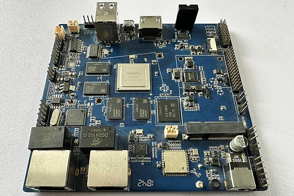
The component list should be reviewed early in the project, before the PCB layout starts. Changing a package after the layout is complete can require a new board, a new stencil, and a new placement program. Early selection avoids expensive revisions.
Role of Package Selection in Design
During product design, the engineer determines the power efficiency and function of the components in the system architecture and detailed circuit design phase. During the SMT design stage, the package form and structure must be selected according to the equipment and process capability.
A surface mount solder joint is both a mechanical connection point and an electrical connection point. It must carry current and also hold the component securely on the board.
Reasonable package selection improves PCB design density, productivity, testability, and reliability. It also reduces the cost of placement, soldering, and rework.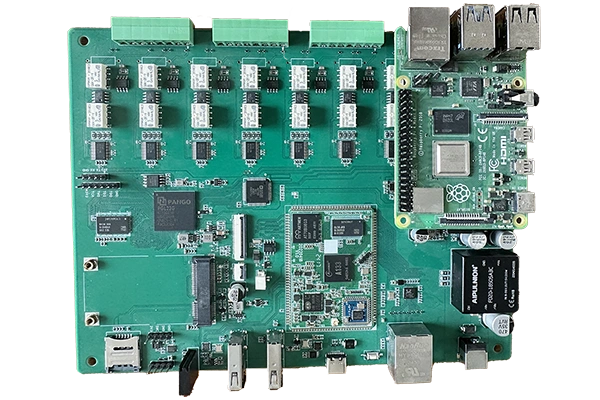
Package Heat Resistance
A surface mount package must survive the high temperature of reflow soldering. If the package material cannot withstand the peak temperature, it may melt, warp, delaminate, or release gas.
The package body and the PCB substrate should have matching thermal expansion coefficients. If one material expands much more than the other, the solder joints can crack during cooling or thermal cycling.
The component supplier should provide the maximum soldering temperature and moisture sensitivity level. The assembly profile should be kept within these limits.
Advantages of Choosing the Right Package
A properly selected surface mount package can effectively save PCB area. Small packages allow the designer to fit more function in a smaller board.
The right package can provide better power efficiency because the signal path is shorter. It also protects the interior of the component from environmental effects such as humidity.
Good packages provide stable communication links and help heat dissipation. They should also be easy to transport, handle, and test during production.
Package selection therefore affects not only the circuit performance but also the manufacturing yield.
Classification of Surface Mount Components
Surface mount components can be divided into two general categories: active and passive. They can also be classified by the shape of their leads, such as gull-wing or J-lead.
Gull-wing leads extend outward and downward from the package body. They are easy to inspect after soldering.
J-lead packages bend the lead under the body, which saves space but makes visual inspection more difficult.
The component type and lead shape should be reviewed together with the placement and inspection capability of the factory.
Passive Component Selection
Passive components mainly include monolithic ceramic capacitors, tantalum capacitors, and thick-film resistors. They are available in rectangular or cylindrical shapes.
The cylindrical passive component is called a MELF. MELF components can roll during reflow soldering and require special liner designs. They should generally be avoided unless the application makes them necessary.
Rectangular passive components are called chip components. They are small, light, resistant to mechanical shock and impact, and have low parasitic loss.
Chip components are widely used in all types of electronic products. To obtain good solderability, the component should have an electroplated nickel barrier finish.
Active Device Packaging
There are two main types of surface mount active device carriers: ceramic and plastic.
Ceramic chip packaging provides good airtightness and protects the internal structure of the component. It also creates shorter signal paths, improving parasitic parameters, noise, and delay characteristics.
Ceramic packages can reduce power consumption. However, the difference in thermal expansion between the ceramic package and the substrate can crack solder joints during soldering if the stress is not absorbed.
The most common ceramic chip carrier used in SMT is the leadless ceramic chip carrier, often called LCCC.
Plastic Packaging
Plastic packaging is widely used in military and commercial products because it offers good cost performance. The main forms are the small outline transistor, small outline IC, plastic leaded chip carrier, small outline J package, and plastic quad flat pack.
The small outline transistor is used for transistors and simple devices. The small outline IC is used for circuits with a moderate number of pins.
Plastic leaded chip carriers and J-lead packages are used when board space is important.
Plastic quad flat packs are used for larger ICs that need many leads around the package body.
Choose the Package Size for the Pin Count
To save PCB area, the designer should choose the smallest package that can satisfy the electrical and thermal requirements. Package size should also match the placement machine capability.
When the device function and performance are the same, an SOIC with fewer than 20 pins is often preferred to a larger package. A PLCC with between 20 and 84 pins may be preferred for moderate pin-count devices.
For devices with more than 84 pins, a PQFP or a BGA may be required. The package should be selected together with the assembly process and the stencil design.
Using the correct package for each pin count reduces board area and improves routing efficiency.
Thermal Expansion and Solder Joint Stress
When the package and substrate expand at different rates, the solder joint absorbs the resulting stress. If the package is large or the CTE mismatch is high, the joint may crack after repeated temperature changes.
The designer should consider the operating temperature range and the thermal cycling requirement of the product. Components used in automotive or aerospace environments need a more stable package and assembly process.
Flexible leads and board-level support can reduce the stress transmitted to the solder joint.
Testing and Reliability Considerations
Package selection affects the testability of the board. Fine-pitch and BGA components may require X-ray inspection because their joints are difficult to reach with optical tools.
Components that are difficult to inspect should be selected only when their benefits clearly outweigh the test cost. The design should provide test points and visible polarity marks where possible.
Component quality should also be verified during incoming inspection. Leads should be flat, solderable, and free from contamination.
A component with a poor finish can reduce the yield of the entire board.
A professional SMT PCB assembly service can help the customer select components that are compatible with the available placement, printing, and inspection processes.
The package library should be reviewed by the PCB design and layout team so that pad geometry and thermal relief are correct.
After assembly, PCBA testing verifies that the selected components function correctly in the final circuit.
A complete PCB assembly process should also use incoming inspection and quality management to prevent component problems from reaching the line.
Supply Chain and Component Availability
Package selection should also consider component availability. A package that is electrically ideal may have a long lead time, a short supply, or frequent allocation risk. The designer should select packages from qualified suppliers and confirm that the component will be available for the complete product life.
Alternate components should be qualified before they are listed in the BOM. The alternate should have the same footprint, thermal behavior, and moisture sensitivity. An unqualified substitute can create a placement or reliability problem even when the electrical specification is similar.
Component packaging for delivery is another supply chain issue. Reels and trays should protect the leads and prevent ESD damage. The component package must also fit the feeder system used by the assembly line.
Moisture and Handling Control
Many surface mount packages are moisture sensitive. The component should arrive in sealed dry packaging with a humidity indicator card. The floor life after the bag is opened should be recorded on the label.
If the floor life is exceeded, the components must be baked before soldering. Baking parameters should follow the package classification and the supplier recommendation. Overbaking can damage the package or degrade solderability.
Handling should protect the leads and the package body. Tweezers, vacuum pickups, and placement nozzles must not bend leads or crack the ceramic body. Static-sensitive components should be handled in an ESD-protected area.
Incoming inspection should verify the part number, date code, quantity, packaging condition, and solderability sample. A small inspection cost at the warehouse prevents a large defect cost on the assembly line.
Conclusion
SMT component selection is a key part of product design. The correct package saves space, improves power efficiency, protects the internal component, and supports reliable soldering.
Passive chip components, ceramic and plastic packages, and lead forms must be matched to the pin count, thermal requirement, and assembly process.
With careful selection, the designer can create a board that is small, efficient, testable, and reliable in production.


