Solder Joint Void Acceptance Criteria Explained
A void is a gap left inside a solder joint where flux volatiles or entrapped air prevented the metal from filling the volume. Voids are present in almost every joint to some degree, so the question is never whether they exist but whether the amount and the position of them are acceptable.
Acceptance is decided by the joint type, by how the joint carries current and heat, and by the standard the product is built to. A void under a thermal pad and a void in a fine pitch signal joint are judged by completely different rules.
How Voids Form
Voids come from three sources: volatiles released by the flux during reflow, air trapped under the paste when it is printed, and outgassing from the surface finish or from plated holes. Each source produces a cavity that the molten solder cannot fill because the gas has nowhere to escape before the joint freezes.
The size and number of voids depend on how quickly the solder solidifies and on how easily the gas can escape. A slow, well controlled profile gives the volatiles more time to leave, while a fast one traps them. Paste with a high solvent content makes the problem worse.
Measuring Voids By X-Ray Inspection
Voids are invisible from the outside, so x-ray inspection is the normal method. A two dimensional image shows the projected void area, while computed tomography builds a three dimensional picture that separates voids at different depths inside the joint.
The measurement is expressed as a percentage of the joint area or volume. Because the technique is a projection, a two dimensional measurement tends to overstate the void fraction in a thick joint, and the method used should be stated whenever a number is quoted.
IPC Criteria And Percentages
IPC criteria differ by joint class and by joint type. For a through hole joint, the usual limit is 25 percent of the cross sectional area, with an additional limit on any single void. For a ball grid array joint, the common limit is 25 percent of the ball area, with voids that intersect the interface treated more strictly.
The criteria are written for a class of product rather than for an individual design. Class 3 criteria are tighter than Class 2, and a product that must pass Class 3 may need a different paste or a different profile from one that only needs Class 2.
Thermal Pads And Their Special Case
A thermal pad is the case where voids matter most, because the joint is the heat path. A void under a power device raises the thermal resistance of the interface, and the resulting temperature rise reduces the life of the component. Limits of 20 to 25 percent are common, and some designs demand less.

The shape of the void also matters. A few large voids are worse than the same total area distributed as many small ones, because a large void blocks the heat path over a significant fraction of the pad. Uniform distribution is the goal, and that is what a good stencil aperture pattern and a controlled profile produce. The way these pads are sized is described under PCB pad design standards.
Reflow Profile And Paste Choices
Reflow profile is the single most effective control. A soak that is long enough to drive off the bulk of the volatiles before the alloy melts removes most of the gas that would otherwise be trapped. A ramp that is too fast reaches liquidus while the flux is still wet and active. Alloy behaviour under these conditions is described under lead-free versus leaded solder.
Paste selection matters as well. A paste with a lower solvent content, a finer powder size and a more active flux generally produces fewer voids, though each of those choices has its own trade off in print quality and in residue.
Reducing Voids In Production
Stencil design is the second lever. Splitting a large thermal pad aperture into a grid of smaller openings lets the flux volatiles escape between the deposits, and the practice is now standard for large pads. The paste volume stays the same while the void content falls.
Other controls include the paste printing parameters, the pad finish, and the amount of time the paste sits on the board before reflow. A joint that is acceptable in the laboratory can fail in production if the paste is left on the stencil too long. How the requirement is agreed with the customer is described under PCBA development process.
Additional Considerations for This Build
Practical attention to solder joint void pays for itself here, because it decides whether the finished board behaves as the drawing intended. Where the requirement is not stated on the fabrication drawing or in the assembly notes, the shop has to assume a default, and that default is rarely the value the design was simulated with. Stating solder joint void explicitly, together with the tolerance that applies, removes the assumption and keeps the result predictable from batch to batch.
Process Control and Verification
On a design of this kind, thermal pad is the item that decides how the rest of the board is arranged. A short note on the drawing about handling, storage or packaging is often worth more than an extra decimal place on a tolerance. Where a value sits close to a process limit, the drawing should say so, since the shop can then open the process window rather than working to a nominal figure that carries no tolerance.
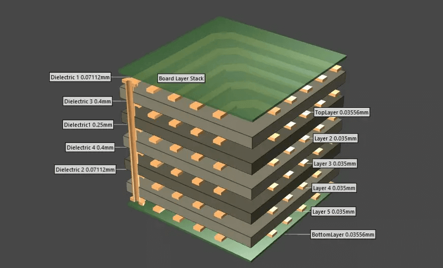
A stack-up that is drawn rather than described removes most of the ambiguity from a quotation, and it lets the fabricator price the board against the dielectric and copper weights that will actually be used. Where the requirement is not written down, the shop supplies its own default, and the default is chosen for the process rather than for the design.
The measurements that matter are the repeatable ones: conductor width and spacing, annular ring, finished hole size, plating thickness and surface finish are all verifiable on a coupon that travels with the panel.
Process Control and Verification
On a design of this kind, thermal pad is the item that decides how the rest of the board is arranged. A short note on the drawing about handling, storage or packaging is often worth more than an extra decimal place on a tolerance. Where a value sits close to a process limit, the drawing should say so, since the shop can then open the process window rather than working to a nominal figure that carries no tolerance.
A first article check confirms that the process and the drawing agree on the points listed above, and that the coupon data supports the values used in the design.
Where a measurement falls outside the expected window, the sample is retained so that the cause can be established before the balance of the batch is released.
FAQ
Does a void always reduce joint strength? Not necessarily. Small, well distributed voids have little effect on mechanical strength, and the concern is mainly thermal and, for high frequency joints, electrical. Large voids at the interface are the ones that matter.
Can voids be repaired? Once a joint is reflowed the only repair is to remove the solder and rebuild the joint. Voids cannot be worked out with a soldering iron, and rework of a ball grid array joint is a specialist operation.
Which standard defines the acceptance limit? The IPC criteria for the joint class, supplemented by the customer drawing. Where the two differ the drawing normally takes precedence and should state the measurement method.