




Solder Mask Developing: 4 Causes of an Uneven Pattern
Solder mask developing is the step that turns an exposed and cured coating into a finished pattern. The developer dissolves the unexposed coating that the artwork left on the pads, and it has to do so completely without attacking the mask that will stay on the board. The window between a clean opening and a damaged sidewall is narrow, which is what makes this stage worth measuring rather than assuming.
It looks like a simple wash, and that is why the step is often set once and left alone. In practice spray pressure, conveyor speed and solution strength all move, and the residue they leave behind shows up later as poor plating, weak solder joints or a mask that lifts at the pad edge.
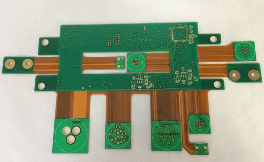
What Solder Mask Developing Does
The mask is applied over the whole panel and then exposed through the artwork. Light cross-links the coating where the mask is wanted, and the unexposed areas over pads, holes and ground windows stay soluble, ready to be washed away by the developer.
A correct cycle leaves a clean copper surface inside every opening, with the mask sidewall standing square and the surface dry of chemical. Anything left behind is a barrier between the copper and the finish that comes next. A clean solder mask developing cycle is judged on three things: bare copper in the opening, a square sidewall and no chemical left on the surface.
Developer Chemistry and Concentration
Aqueous developers are usually dilute solutions of sodium or potassium carbonate, chosen because they dissolve unexposed coating quickly while attacking cured mask very slowly. The concentration is set by titration, and the working range is narrow enough to need routine checks. Carbonate is also consumed as it neutralises the acid groups in the coating, so the titration falls for two reasons at once.
A weak developer leaves a film of unexposed coating over the copper, while an over-strength bath attacks the cured sidewall and undercuts the edges. Because the bath loads with dissolved coating as panels pass through it, the concentration falls during a shift and must be brought back to target.
Spray Pressure and Nozzle Pattern
Spray pressure decides how hard the developer hits the panel, and it has to be enough to flush dissolved coating out of small openings but gentle enough not to damage the mask that stays. The pattern from every nozzle must overlap its neighbour, or a stripe of unremoved coating follows the panel down the line.
Nozzles wear and block, so the pattern degrades gradually and unevenly. A blocked nozzle is one of the most common causes of a localised residue defect, and oscillating spray bars exist to keep the coverage even along the conveyor. Checking the pattern on a glass plate once a week is the simplest way to catch a bar that has drifted out of alignment.
Conveyor Speed and the Breakpoint
The conveyor speed sets the dwell in the developer and, with it, the breakpoint, the point along the chamber where the coating finally clears. The breakpoint should sit inside the chamber with enough length left for the remaining developer to work and for the rinse to follow.
A speed that is too high pushes the breakpoint past the end of the chamber, so panels leave partly developed. A speed that is too low over-develops the mask and widens the openings beyond the artwork, which shows later as exposed trace edges or solder bridging. The breakpoint can be watched through the chamber window, and moving it is the quickest correction available to the operator.
Rinse and Residue Removal
The rinse that follows the developer has two jobs: remove the dissolved coating and stop the developer from continuing to act. Spray rinse at the exit does the first, and a pH check on the final rinse water confirms that the second has been achieved.
Rinse water carried forward from the developer stage also dilutes the bath, so the plumbing must keep the two apart. Residue on the panel is easiest to see under UV light, where unremoved coating fluoresces against the copper underneath. Where the rinse is recirculated, conductivity should be logged alongside the pH so that a change in water quality is visible.
Tank Loading and Solution Life
The developer bath has a finite capacity for dissolved coating. Every panel adds solids, and once the solution is loaded it loses the ability to open a fine pattern, even when a titration suggests the active content is still adequate.
Solution life is therefore planned from the loading figure, not from the calendar, and the bath is dumped and remade at a defined number of square metres. Filtration helps in some lines but does not remove dissolved solids, so it cannot extend the life of the charge. A solder mask developing bath run past its loading limit fails on fine openings long before it fails on coarse ones.
Undercut, Over-Development and Edge Quality
Undercut is the sideways removal of mask under the edge of the opening, and it follows from too much dwell or too strong a developer. Undercut also grows as the developer loads, so the same bath can hold the edge quality in the morning and lose it by the end of the shift. A small amount is normal and tolerable, but a growing undercut narrows the mask dam between adjacent pads.
On fine-pitch patterns that dam decides whether solder can bridge during assembly. Development is therefore judged on the finished sidewall and on the pad opening, and the judgement is made from a microsection or from a measurement under a microscope.
Symptoms of Poor Development
The visible symptom is residue, a haze or a scum on the copper inside the opening rather than loose coating. Solder will not wet a pad that carries it, and finish baths will not plate it, so the defect is usually found at electrical test or in the assembly house.
The opposite symptom is an opening that is visibly wider than the artwork, with a soft, sloping sidewall and a mask dam that has been eaten back. Both kinds of defect trace back to the same three variables: chemistry, spray and speed, and all three belong in the solder mask developing record.
Verification and Records
Verification starts with a first-article panel inspected under UV and under a microscope after solder mask developing, followed by a check of the pH of the final rinse. The exposure energy that set the pattern is confirmed separately, as described in exposure energy control.
The record should carry the developer concentration, the spray pressure, the conveyor speed and the rinse readings for each lot. Where the mask has been pre-cured, the condition of the coating entering the developer comes from solder mask pre-cure control, and the copper surface underneath is prepared as described in copper surface preparation. Test methods follow the IPC guidance published by IPC.

FAQ
Why does residue appear only in some areas of the panel? Localised residue usually points at a blocked or worn nozzle or at a spray bar that does not overlap correctly, rather than at the chemistry.
Can developer concentration be checked by titration alone? Titration shows active content, but it cannot show dissolved coating. A loaded bath can titrate correctly and still fail to open a fine pattern.
How much undercut is acceptable? The limit follows from the fine-pitch dam on the design. It should be measured on a sample and stated in the process specification rather than judged by eye on the line.



1 Comment
Solder Mask Tack Cure: 6 Settings For A Stable Surface
[…] well, since a mask that develops slowly may be under-cured rather than over-developed. Our note on solder mask developing control covers the other half of that interaction. Acceptance criteria for the finished mask, including […]