Solder Mask Over Via: Process, Design Rules and Cost
Why Solder Mask Over Via Matters
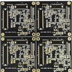
In modern printed circuit board manufacturing, even a small detail can change the reliability, performance and cost of the final product. Solder mask over via, often called SMOV, is one of those details. It is the process of covering a via completely with solder mask so the hole is sealed and the surface stays clean. With electronics moving toward higher density and smaller form factors, engineers and buyers need to understand when to use SMOV and how to design for it.
This guide explains the SMOV process, the difference between a covered and an open via, the design rules that control quality and the cost trends in 2026, so you can make a practical decision between tenting, opening and plugging your vias. In every case the goal is the same: a board that solders well and keeps working for years.
What Is a Via?
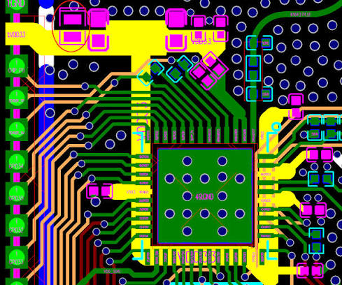
A via is a small plated hole that carries electrical signals between the layers of a multilayer circuit board. It is the backbone of complex routing. The three common types are through hole vias that pass through every layer, blind vias that connect only an outer layer to an inner layer and buried vias that connect only inner layers. Vias distribute power and ground, connect signal layers and make high density routing possible.
What Is a Solder Mask?
The solder mask is the protective coating applied over the copper surface of a board, usually green but available in other colors. It prevents solder bridges during assembly, stops copper from oxidizing or corroding, improves insulation and adds mechanical strength. Common types are liquid photo imageable solder mask, dry film solder mask and epoxy solder mask.
What Is Solder Mask Over Via?
Solder mask over via is the manufacturing treatment that covers a via completely with solder mask, so no copper is exposed on the board surface. The via is fully sealed and, for small vias, the mask normally bridges over the hole because the opening is not much larger than the hole itself.
The main difference is simple. An SMOV via is sealed and protected, while an open via is exposed and can oxidize or wick solder during assembly. For signal vias that do not need to be soldered, covering them is the most economical way to stop contamination and keep the surface flat.
SMOV vs Via Opening
Solder mask over via (SMOV). The via is completely sealed under the solder mask. There is no bare copper and no risk of contaminant entry or solder wicking. It suits small vias and boards that need a flat, clean surface. The tradeoff is that larger vias can be difficult to cover completely, and a covered via cannot be used as a test point or a soldering pad.
Via opening. The pad and hole are left exposed so solder can wet the copper. It is needed for through hole components, test points and any connection that must be soldered. Exposure means the hole can trap flux, moisture and dust, and a large opening increases the chance of solder wicking during reflow.

The SMOV Process
SMOV starts with the same steps as any solder mask application. The board is cleaned and the copper surface prepared, then liquid or dry film solder mask is applied over the whole panel. In the imaging step the artwork keeps mask over the vias instead of opening it, so the via is covered instead of exposed. After exposure and development, the mask is cured at high temperature to form a hard protective layer. Finally the board is inspected to confirm the vias are covered without blistering, bleed or voids.
The most sensitive point is the relationship between the via size and the soldermask opening. If the via is too large or the drill tolerance too loose, the mask may sag into the hole or fail to seal it. A good fabricator controls drill size, annular ring and soldermask registration together so the coverage stays uniform.
Design Rules for SMOV
Keep vias small enough for the mask to bridge consistently. In practice vias under about 0.3 mm form a reliable tent, while larger vias may need a plug first. Leave a small annular ring around the via so the mask has copper to adhere to, and make sure the drill and the artwork come from the same data so the hole stays centered under the opening. Confirm the final board uses an adequate solder mask thickness and a cure profile that avoids cracking on the thin tent, and coordinate the stack up with a PCB design and layout review.
Benefits and Limitations of SMOV
Benefits. SMOV keeps the surface flat for solder paste printing, stops contamination and corrosion, prevents solder from wicking into the via during assembly and avoids short circuits between adjacent solder joints. It is cheap because it uses the existing solder mask, and it protects signal vias at almost no extra cost.
Limitations. A covered via cannot be used as a soldering pad or a test point, and very large vias are hard to tent reliably. If the mask thins or sags, voids and cracks can appear. For high reliability boards that need a hermetic seal or a via in pad, a plugged via is the stronger choice.
SMOV Cost in 2026
SMOV adds little to the board cost because it uses the solder mask step that is already required. The real cost driver is not the coverage but the board itself: layer count, via count, via size and surface finish. A two layer board with simple SMOV vias stays inexpensive, while a dense multilayer board with many small vias costs more per square centimeter.
In 2026 a standard board with solder mask over via typically adds only a small premium over an open via board. If the design needs a plugged via for every hole because the vias are large or the product demands it, the price rises because each via must be filled. For high volume production the cost per board drops and the small SMOV premium becomes negligible.
Because the real price depends on the panel size, layer count and via density, a quote that includes those parameters gives a better estimate than a flat per board figure.
Common SMOV Problems
Mask sagging into the hole. Caused by a via that is too large for the mask to bridge. Reduce the via size or switch to a plugged via.
Blistering or bubbles. Caused by moisture or poor surface preparation before mask application. Improve cleaning and dry the board before processing.
Cracking over the via. Caused by a brittle mask or an incorrect cure profile. Use a flexible solder mask and follow the recommended cure schedule.
Coverage miss. Caused by misregistration between the drill and the artwork. Align the data so the via stays centered under the opening.
FAQ
What is solder mask over via? It is the process of covering a via completely with solder mask so the hole is sealed and the surface stays flat.
What is the difference between SMOV and via opening? SMOV seals the via, while via opening exposes the pad and hole so it can be soldered or probed.
When should I use a plugged via instead of SMOV? Use a plugged via for large holes, via in pad designs and products that need a hermetic seal or a very flat surface.
Can I probe an SMOV via? No. A covered via cannot be used as a test point, so place test points on pads that are opened.
Get a Reliable Solder Mask Over Via Design
SMOV is one of the cheapest ways to protect signal vias and keep the board surface clean, but it only works when the via size, annular ring and solder mask registration are controlled together. Pair it with PCB manufacturing expertise and verify the result with PCBA testing before a board ships. Contact gopcb for design support, stack up review and a solder mask over via quotation for your next project.