
Solder Mask Registration: Design Rules and Process Limits
Solder mask registration is the offset between where the mask opening was drawn and where it lands on the copper, and it is the reason a drawing that looks comfortable can still produce exposed copper on one side of a pad and a covered pad on the other. The tolerance is a stack-up of drill, imaging and process allowances, and it has to be compared against the pad clearance the design actually offers.
Why Registration Offset Exists
Mask artwork is imaged from the same data as the copper, but the two are produced in different steps with different tooling. Copper is etched after imaging, the mask is printed or laminated and then exposed, and the panel moves between machines. Each step contributes a small displacement, and the sum appears as an opening that is shifted relative to the pad it is meant to expose.
Panel scale change adds to the effect. Laminate that grows during lamination and shrinks during cooling moves the copper pattern relative to the tooling holes, so an opening that is centered on one panel may be offset on another from the same lot. This is why registration is specified as a tolerance rather than as a single value. Panel scale change of 0.02 percent across a 500 mm panel moves features by 0.1 mm, which on its own can consume the whole registration allowance on a fine-pitch design.
What the Tolerance Stack Contains
A realistic registration tolerance combines imaging position, etching bias, mask exposure position, and the movement of the panel itself. A common allowance is plus or minus 0.075 mm for a standard process, tightening to about plus or minus 0.05 mm on fine-pitch work with better tooling. These numbers should be on the fabrication drawing rather than assumed.
The tolerance applies around the full perimeter of the opening, not to the center. An opening that is correctly positioned at its center can still clip a corner of a pad if the aperture is slightly small, which is why the check is made on the smallest remaining mask web rather than on the nominal offset.
Dam Width and the Limit of Shrinking Openings
The dam width between two adjacent openings has a practical floor, because a web of mask that is too thin will not survive development, will lift during reflow, or will break and bridge. Below roughly 0.075 mm the web becomes unreliable, and below 0.05 mm it should not be assumed at all on a volume product. The dam is what forces a design to resolve tight pitch on the copper rather than on the mask.
When the pitch is fixed and the dam cannot shrink, the opening has to shrink instead, which eats into the annular clearance. That is the point at which the mask starts to cover the pad edge and the assembly process begins to see solder starvation and poor wetting on one side of the joint.
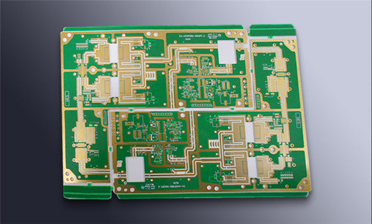
The Mask Opening to Pad Clearance Rule
The usual rule is that the mask opening should be 0.05 to 0.10 mm larger than the pad on every side, so the opening clears the copper even when registration is at its worst and still leaves a web where the design needs one. Larger openings expose laminate between pads, which collects flux and can bridge; smaller ones clip the pad and reduce the wettable area.
The clearance is applied per side, which means a 0.05 mm rule adds 0.1 mm to each dimension of the pad. On a 0.4 mm pad this is a 25 percent increase, and on a 0.2 mm pad it doubles the opening. Below about 0.25 mm pad size the rule has to give way to a tighter registration specification rather than to a smaller clearance.
Openings Over Vias and Fiducials
Vias that must stay sealed need a mask tent that is at least 0.15 mm larger than the via on every side, which is a registration requirement as much as a design one. Where registration is loose, a tent that is marginal on the drawing becomes an exposed via on the panel, and the failure does not appear until the board sees flux or cleaning chemistry.
Fiducials have the opposite requirement: the mask opening must expose the whole fiducial with a clear border, because a partially covered fiducial gives the vision system a false centroid and shifts placement for the whole panel. As with pads, the clearance is added per side, and the border must survive worst-case registration.
Copper-to-Mask and Copper-to-Edge Interactions
Where copper runs close to the board edge or to a mask opening, the mask has to be able to cover it. A trace that is nominally covered but sits within the registration tolerance of the opening can be exposed at the edge of the opening, which presents bare copper in a place the design assumed was protected, and that is where corrosion and solder bridging start.
The check is geometric rather than chemical: take the opening, add the registration tolerance in the worst direction, and see whether any conductor that must remain covered falls inside. If it does, the fix is a design change, and it is much cheaper at the layout stage than as a fabrication waiver.

Design Rules That Keep Registration Workable
Keep pad-to-pad spacing consistent, avoid mixing a tight-pitch area with a coarse one if the mask process cannot serve both, and use the same registration class across the panel. Mixed requirements force the shop to build to the tightest rule everywhere, which costs money and often produces a conservative result that still misses somewhere on the panel.
Where the design cannot avoid a marginal rule, mark it and specify the measurement. A note that asks for registration verification on the specific features at risk is far more useful to a fabrication shop than a global tolerance that says nothing about which features matter.
Verifying Registration on the Fabricated Panel
Registration is verified by measuring the mask web or the exposed copper at several points across the panel, not by looking at one location. Measure the smallest web and the largest offset, then compare both against the drawing. Because panel shrink varies across the sheet, sampling a single corner can show a comfortable margin while the opposite corner is out of specification.
For high-reliability work, record the measurements against panel location so a pattern of drift across the sheet is visible. A consistent gradient points to lamination or exposure tooling, while a random scatter points to handling and positioning.
What Registration Failure Looks Like Downstream
Exposed copper at a mask opening shows up as solder bridging between pads, as corrosion in a humid environment, and as poor coating adhesion where a conformal film has no mask to key to. Clipped pads show up as insufficient solder and as weak fillets on one side of a joint. Each of these is diagnosed during assembly as a process problem when the root cause was on the mask artwork.
That misattribution is expensive, and the way to avoid it is to qualify registration at incoming inspection on the first lot rather than after a defect appears. The mask measurement takes minutes, while a bridging investigation on a dense board can consume days.
FAQ
What registration tolerance should be specified? About plus or minus 0.075 mm for a standard process, tightening to roughly plus or minus 0.05 mm on fine pitch. The value belongs on the fabrication drawing.
How much larger should a mask opening be than the pad? Typically 0.05 to 0.10 mm per side, so the opening clears the copper at worst-case registration without exposing laminate between adjacent pads.
What is the minimum practical mask dam? Roughly 0.075 mm on a volume process. Below 0.05 mm the web is unreliable through development and reflow and should not be assumed in a design.