Thermal Relief Design Rules for Plane Connections
A pad connected directly to a copper plane is thermally welded to it. That is excellent for current capacity and for heat spreading, and it is a problem for soldering, because the plane draws energy away from the joint faster than any soldering process can supply it. A thermal relief resolves the conflict by connecting the pad through narrow spokes, trading a little electrical and thermal performance for a joint that can be made reliably.
What a Thermal Relief Is
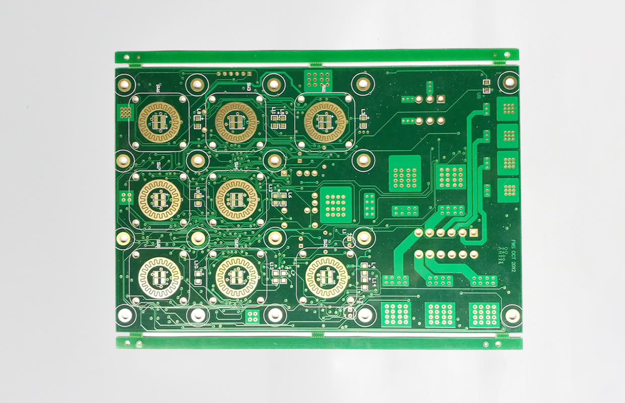
A relief is a pad connected to the surrounding plane by three or four narrow bridges, with the rest of the perimeter separated by a clearance ring. The pad is still grounded, but the path between the pad and the plane has a much smaller cross section, which limits the rate at which heat can flow away during soldering.
The clearance ring is usually the same width as the mask expansion, and the spokes are typically 0.2 to 0.5 millimetres wide. Both values are chosen for the process rather than for the electrical circuit, which is why they belong in the fabrication and assembly notes as well as in the layout.
Why Soldering Needs It
Soldering heat has to raise the pad and the joint above the liquidus of the alloy. A plane connected pad conducts that heat away in every direction at once, and on a thick copper layer the effect is strong enough that a hand soldered joint never reaches temperature, or an oven profile that works for the rest of the board leaves this joint cold.
The relief reduces the heat flow to a rate the process can overcome. The result is a joint that forms in a normal time and at a normal temperature, which is what allows the profile to be set for the whole board rather than for one pad. Our note on reflow oven profile verification describes how the effect is confirmed.
Spoke Width and Count
Four spokes are the usual choice. Three also works but leaves the pad slightly asymmetric, and two spokes halve the current path without a corresponding benefit. More than four brings the thermal performance close to a solid connection while making the pad harder to route.
Width is the parameter that actually sets the trade. Wider spokes carry more current and conduct more heat, narrowing them improves soldering and reduces the current path. For a power pad the relief may be inappropriate altogether, and the joint is then made with a longer preheat rather than with a narrower connection.
Current and Thermal Performance
A relief raises the resistance between the pad and the plane, and the effect is small for a signal connection and significant for a power one. Where the pad carries a heavy current, the spokes should be sized by the same calculation as any other conductor, and the current capacity guidance in our article on high current capacity applies.
Heat spreading is affected in the same way. A relieved pad conducts less heat into the plane, which matters where the plane is being used as a heatsink for the component. Where it does, the trade is a decision between assembly yield and operating temperature, and the analysis in our article on thermal management design is the right framework for it.

Vias Inside Pads and Reliefs
Vias placed in a pad are often used to carry heat from a component into the plane, and they conflict with the relief in the same way a solid connection does. A hot pad with many vias behaves thermally like a solid plane connection, and the soldering problem returns even though the pad itself is relieved.
Where vias in pads are necessary, they are normally filled or plugged so that they do not draw paste away, and the heat path is accepted as part of the design. The combination should be reviewed as a single decision rather than two independent ones.
When Not to Use a Relief
A solid connection is the correct choice where the joint must carry a high current, where the pad is a thermal path into the plane, or where the pad will be soldered by a process with ample energy such as selective soldering with preheat. It is also correct where the pad is not soldered at all, such as a mounting hole or a test point.
The mistake is to apply one rule to every pad. A design that relieves a power pad to make soldering easier may create a hot spot, and a design that solidly connects every ground pad may create a joint that never forms. The rule should be applied by function.
Effects on Inspection and Rework
A relieved pad heats and cools faster than a solid one, which changes how the joint looks after reflow. That is why a board where some pads are relieved and others are not can show a variation in fillet appearance that is a consequence of the layout rather than a defect.
Rework is easier on a relieved pad, because less energy is required to reach temperature and the surrounding laminate heats less. Where a board is expected to see repair, that is a genuine argument for relieving the connections on the parts most likely to be replaced.
Documenting the Choice
The fabrication notes should state the spoke width, the clearance and the pads to which each applies, and the assembly notes should record any pad where a solid connection was chosen and why. That record is what allows a later review to distinguish a deliberate choice from an oversight.
Where the profile is unusual because of a thermal mass on the board, the reason should be recorded with the profile. The judgement framework is the same as any other quality decision, and the principles in our article on PCB quality assessment apply to the documentation as much as to the board.
Additional Considerations for This Build
Practical attention to layout rules pays for itself here, because it decides whether the finished board behaves as the drawing intended. Where the requirement is not stated on the fabrication drawing or in the assembly notes, the shop has to assume a default, and that default is rarely the value the design was simulated with. Stating layout rules explicitly, together with the tolerance that applies, removes the assumption and keeps the result predictable from batch to batch.
Deliberate attention to solderability pays for itself here, because it decides whether the finished board behaves as the drawing intended. Where the requirement is not stated on the fabrication drawing or in the assembly notes, the shop has to assume a default, and that default is rarely the value the design was simulated with. Stating solderability explicitly, together with the tolerance that applies, removes the assumption and keeps the result predictable from batch to batch.
Process Control and Verification
On a design of this kind, solderability is the item that decides how the rest of the board is arranged. A short note on the drawing about handling, storage or packaging is often worth more than an extra decimal place on a tolerance. Where a value sits close to a process limit, the drawing should say so, since the shop can then open the process window rather than working to a nominal figure that carries no tolerance.
FAQ
Can a thermal relief be omitted on a ground pad? It can, and sometimes should be, but the profile then has to supply enough energy for that joint. Relieving is the simpler answer where the current does not require a solid connection.
How wide should the spokes be? Between 0.2 and 0.5 millimetres for typical boards, sized upward for current carrying pads. The value should follow the function rather than a default.
Does a relief affect impedance? On a controlled impedance net the reference plane connection matters, so a relief on a via or pad in the return path should be reviewed. The effect is usually small but is not always negligible.