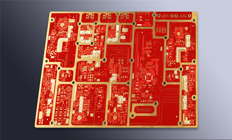
Three-Stage Design Review Before Gerber Release
A layout error is one of the few engineering mistakes that cannot be corrected in software. A trace that carries the wrong net, a via placed where it destroys a return path or a footprint that does not match its component all leave the design stage looking complete and reappear as a bare board that has to be cut, strapped or scrapped. This is why the design review is a process rather than a final glance, and why it is structured in stages that look for different classes of fault.
The principle behind the structure is simple: quality is not filtered at the end but accumulated through the work, and each stage is aimed at the faults the previous one is least likely to catch.
Why One Review Pass Is Not Enough
A single review tends to be either too detailed or too general. An engineer reading a layout closely enough to check every trace width will miss the systemic question of whether the power distribution can supply the current the design needs; an engineer looking at the architecture will not notice a misplaced reference designator. Separating the passes allows each one to be performed at the right level, by someone with the right distance from the work.
Distance matters most. The engineer who drew the board knows what each trace is supposed to do and unconsciously reads the intended design rather than the drawn one. That is the fault the second stage exists to remove.
Stage One: the Self Check Against a Checklist
The first pass is the designer’s own, performed against a written checklist rather than from memory. A checklist of eighty or more items covering power and ground connectivity, trace width against current and impedance, spacing, via specification, silkscreen and mechanical dimensions turns a general intention to be careful into a set of confirmations that are either done or not.
The value of the list is that it does not depend on the day. A self check on a quiet afternoon and a self check on the day before a release produce the same result, because the items do not change and the answers are visible in the file. Most of what this pass catches is inexpensive to fix and would be embarrassing to find later: a net that was never connected, a pad that belongs to the wrong package, a component whose orientation legend contradicts the assembly drawing.
Manufacturability and DFM belong in this pass as well, in their first form. Minimum annular ring, drill sizes against the fabricator’s available tooling, copper to edge clearance and solder mask sliver width are all visible at this stage, and all of them are cheaper to change now than after the panel has been made.

Stage Two: Cross Review by Another Engineer
The second pass is a cross review by an engineer who did not work on the design. Their advantage is not greater skill but the absence of assumption: they read the board as drawn. This is the stage that catches the logical faults — topology that does not match the interface standard, length matching that was never completed, a high speed signal crossing a split in its reference plane, a plane that is too narrow to carry the return current it will see.
Power distribution is examined here in the same way. Whether a plane or a trace can deliver the current without an unacceptable rise, whether a change of reference plane is accompanied by a return path stitch, and whether the decoupling is placed where it can act rather than where it fits are all questions that require reading the board as a whole.
Thermal and mechanical questions are also raised at this level, because they are easy to see from outside and easy to overlook from inside: a part that cannot dissipate its heat into the copper available, a connector that cannot be reached by its cable, a component that collides with the enclosure or with the tooling that will assemble it.
Stage Three: Senior Sign-Off on Systemic Risk
The last pass is performed by an engineer with a decade or more of experience, and it deliberately avoids detail. Signal integrity is judged at the level of the stack-up and the impedance strategy, the power distribution at the level of whether the current requirements can be met under the worst case, and electromagnetic behaviour at the level of loop area, filtering and shielding.
This pass is also the one that matches the design against the factory that will build it. A design is only manufacturable in the context of a specific capability envelope, and the final review confirms that the minimum features, the layer structure and the finishes assumed in layout are the ones the fabricator can actually hold.

How Findings Are Graded
Not every finding stops a release, and treating them as if they did would make the process unusable. Findings are graded instead. A fault involving electrical connectivity, a shorted supply or a failed signal integrity requirement is a blocking item: the design does not leave the stage until it is corrected. A finding that affects manufacturability or long term reliability is raised with the customer and resolved by agreement, because the correct answer may depend on a cost or schedule decision only the customer can make. A suggestion that does not affect function is recorded as advice, so that the designer can weigh it without being forced to act on it.
The grading is what keeps the reviews credible. If a review that finds nothing wrong is treated as suspicious and a review that finds something trivial is treated as a failure, engineers stop reporting accurately, and the process degrades into a signature.
The Standards Behind the Checks
The checks are only as good as the criteria behind them. Electrical rules such as trace width, spacing, via specification and impedance derive from the design standard and from the customer’s own process requirements. The manufacturability checks derive from the specific capability of the partner factory, which is why a generic rule of thumb is not enough. Signal integrity checks derive from the interface standard and from whatever simulation was performed. Electromagnetic checks derive from general design practice around loop area, filtering and shielding.
All of this sits alongside other controls, including quality management certification and the process records that accompany an order. The design work itself is performed as PCB design and layout, the envelope it must respect is published as PCB capabilities, the build that follows through PCB manufacturing, and the assembly that puts the parts on the finished board through SMT assembly.
Records and What They Are For
Every review is recorded, including the findings that were resolved and the ones that were graded as advisory. The immediate purpose is traceability: if a question is raised months later about why a particular decision was made, the answer exists rather than being reconstructed.
The second purpose is improvement. A finding that recurs across projects is a finding that belongs in the checklist, and the checklist is only useful if it grows. That feedback is what turns the experience of individual engineers into something the organisation retains.
FAQ
How many reviews does a design go through? Three: the designer’s own check against a checklist, a cross review by another engineer and a senior review focused on systemic risk.
Does every finding block the release? No. Findings are graded, and only those affecting electrical function or a defined signal integrity requirement block the release outright.
Why review against a specific factory? Because a design is manufacturable only within a capability envelope, and the limits that matter are the ones the factory can actually hold.