UPS Circuit Board Design: Inverter, Charger and Layout
A UPS circuit board sits between the mains supply and equipment that is not allowed to stop, so it has to handle high voltage, high current, thermal cycling and continuous operation at the same time. The topology chosen at the start decides how the board is laid out, how much copper it needs and how the safety clearances are drawn. This guide follows the main architectures and the layout consequences that come with each.
The Main UPS Architectures
Standby or offline units pass mains through to the load while the supply is healthy and switch to inverter output when the input falls outside its window. Line-interactive units add a tap-changing transformer that corrects moderate voltage deviations before the inverter is called on, which reduces battery cycling.
Online double-conversion units rectify the incoming supply and rebuild the output continuously from the DC bus, so the load never sees a transfer. Delta-conversion designs inject a compensating voltage in series with the mains instead of converting the whole load, which suits large installations where efficiency matters as much as protection.
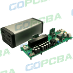
<img src="https://www.gopcba.com/wp-content/uploads/2020/12/project_image_08-1.jpg" alt="UPS circuit board with inverter stage and battery charger section” />
Line-Frequency Versus High-Frequency Design
The distinction is the switching frequency of the converter and its transformer. A line-frequency machine operates the transformer at the mains frequency, so the magnetics are large and heavy but thermally robust and simple to control. A high-frequency machine switches in the tens of kilohertz, which shrinks the transformer and the filter.
The board-level consequences are significant. High-frequency designs need tight gate loops, carefully placed decoupling and attention to radiated noise, while line-frequency designs need large copper areas for current and generous thermal paths. Both have to meet the same safety standard, and the safety clearance rules do not relax with frequency.
Rectifier, Power Factor Correction and DC Bus
The front end converts the mains to a DC bus, and in most modern designs it includes power factor correction so that the current drawn is close to sinusoidal. The PFC stage is a boost converter, which means the switching node is a high dv/dt source sitting next to a sensor that measures the input current.
Layout here follows the same discipline as any other switching supply. Keep the high-current loop small, return the gate drive to the source of the switch, and route the current sense as a Kelvin connection. Rules that apply to a dc-dc converter apply here as well, only with more voltage and more copper.
Inverter Stage and Gate Drive
The inverter turns the DC bus back into an alternating output, using a bridge or a half bridge with a transformer depending on the topology. Each switch carries the full load current, so the copper feeding the bridge is sized by current calculation rather than by habit.
Gate drive routing deserves particular care. The loop from driver to gate and back to the emitter must be short and free of shared return, because any inductance in that loop slows the transition and raises switching loss. Where a bridge is used, the high side and low side drivers should be placed to keep both loops compact and symmetric.
Battery Charger and DC Link
The charger converts the DC bus down to the battery voltage and has to control current as well as voltage. Its layout is a second switching supply on the same board, and the most common mistake is to let its return current share a path with the inverter return, which couples switching noise into the charging control loop.
Battery terminals carry high current and are frequently connected and disconnected, so the copper between the connector and the switching devices should be short and wide, with sense lines taken from the pad rather than from the end of a trace. Contact resistance in the connector is a real thermal source and should be treated as one.
Clearance, Creepage and Isolation
Safety requirements set the minimum creepage and clearance between the mains side and the output, and between primary and secondary in any isolated stage. These distances depend on the working voltage, the pollution degree and the insulation group of the board material, so they must be taken from the standard rather than guessed.
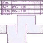
Slots cut into the board are a legitimate way to increase creepage without adding distance, and they are common under opto-couplers and transformers. The isolation barrier should be obvious in the layout, with a clean strip of empty board and no traces crossing it except through the approved isolation device.
Thermal Design and Reliability
Power boards fail thermally more often than electrically. Losses are concentrated in the switching devices, the magnetics and the connector contacts, and the copper under those parts is part of the heatsink. Using power trace planning deliberately, with thermal vias under surface-mount devices and generous copper, spreads the heat into the board.
Derating is the other half of reliability. Running switches near their voltage and current limits shortens life, and electrolytic capacitors on the DC bus age faster at high temperature. Leaving margin on both makes the difference between a unit that survives one outage and one that runs for years.
Control, Sensing and Protection
The controller has to measure input voltage, output voltage, load current and battery state at the same time, and every one of those measurements is a small analogue signal living next to a large switching current. Separating the sense returns from the power returns is what keeps the readings usable.
Protection circuits are laid out around the same principle. Over-current detection needs a fast path to the gate driver so the bridge can be shut down before the devices are damaged, and that path should be short and direct rather than routed through the quiet corner of the board.
Mechanical and Assembly Considerations
These boards are heavy in copper, so they are also heavy to handle. Heavy copper layers affect the minimum trace and space that a fabricator can hold, and they change the drilling and plating process, which is why the copper weight should be declared rather than assumed.
Assembly follows from the same facts. Large magnetics and connector blocks transfer mechanical load to the solder joints, so mounting and stiffening points belong in the layout, and the placement of the heavy components should be checked against the enclosure and the cable routing before the design is released.
Documenting the topology is part of the design work rather than an afterthought. A drawing that names the stages, the switching frequency and the isolation barrier saves the fabricator and the assembly house from inferring intent, and it makes the safety distances verifiable by inspection instead of by assumption.
FAQ
What is the difference between an offline and an online UPS? An offline unit switches to inverter output when the mains fails, so the load sees a short transfer. An online unit converts continuously and never transfers, which is why it is used for sensitive equipment.
Why do high-frequency UPS boards need different layout rules? Because the switching edges are much faster. Gate loops must be shorter, decoupling closer and noise containment tighter, even though the safety clearances stay exactly the same as on a line-frequency board.
Which part of a UPS circuit board causes the most failures? Thermal fatigue. Switching devices, magnetics and battery connectors concentrate losses, and electrolytic capacitors on the DC bus degrade with temperature, so derating and copper heat spreading decide the service life.