USB Cable Shielding and EMC in Industrial Instruments
An industrial instrument with a USB port for configuration and data transfer is exposed to an environment that the interface was never designed for. Motor starting, variable frequency drive harmonics, and relay arcs all produce conducted and radiated disturbance on the same panel, and a link that works on a desk can drop out repeatedly in the field. The failures are usually intermittent, which makes them expensive to diagnose after installation.
The differential pair that carries the data has some natural immunity to common mode interference, because the receiver responds to the difference between the two conductors. That immunity is finite, and the disturbance levels in an industrial cabinet exceed what the interface assumes. When the edges are distorted enough that the receiver cannot resolve them, the result is a checksum error and a retransmission, or a lost connection that re-establishes when the cable is unplugged and reinserted.
What Makes the Industrial Environment Different
Office equipment operates near a handful of low power switching supplies. An industrial panel can contain drives switching hundreds of amperes, contactors that produce fast transients when they open, and long cables that act as antennas for everything in the cabinet. The interference arrives both as a conducted disturbance on the supply and as a radiated field, and USB cable shielding has to address both rather than the differential pair alone.
Timing is the other difference. USB transfers data in frames with tight timing relationships, and a disturbance that shifts an edge by a fraction of a bit period can corrupt the frame. That is why the symptom is usually a retry rather than a total failure, and why an intermittent fault that appears only when a nearby machine starts is a shielding and grounding problem rather than a software problem.
Shield Structures and What Each Layer Does
A cable shield is usually built from two materials for two reasons. A foil layer provides close to full coverage of the conductors and is effective against high frequency fields, because the continuous conductive surface presents a low impedance to the currents the field induces. A braid over the foil adds mechanical strength and handles lower frequencies, where the skin depth is greater and a solid conductor is less important than a low resistance path.
For severe environments the structure can be extended to a double braid over foil, which improves both the coverage and the current carrying capability of the shield at the cost of diameter, flexibility and price. The twisted construction of the data pair matters independently of the shield: a uniform lay length keeps the coupling to the environment balanced between the two conductors, so the disturbance appears as common mode voltage that the receiver rejects, rather than as a differential error.
Termination Decides Whether the Shield Works
A shield only diverts interference if the current it carries has somewhere to go through a low impedance path. That is why shield termination is as important as shield coverage. The best practice is a circumferential connection between the shield and the connector shell around the full perimeter, which presents a very low impedance at high frequency. A short pigtail wire soldered from the shield to a pin may look equivalent at low frequency, but its inductance rises with frequency and it becomes ineffective exactly where it is needed.
Where the shield is connected and how many times also matters. For USB the shield is normally bonded at the host end, with the device end arranged so that the common mode current returns through a defined path rather than through the signal pair. The objective is not to eliminate ground potential differences, which is impossible, but to keep the resulting common mode current away from the data conductors.
What the Board Can Contribute
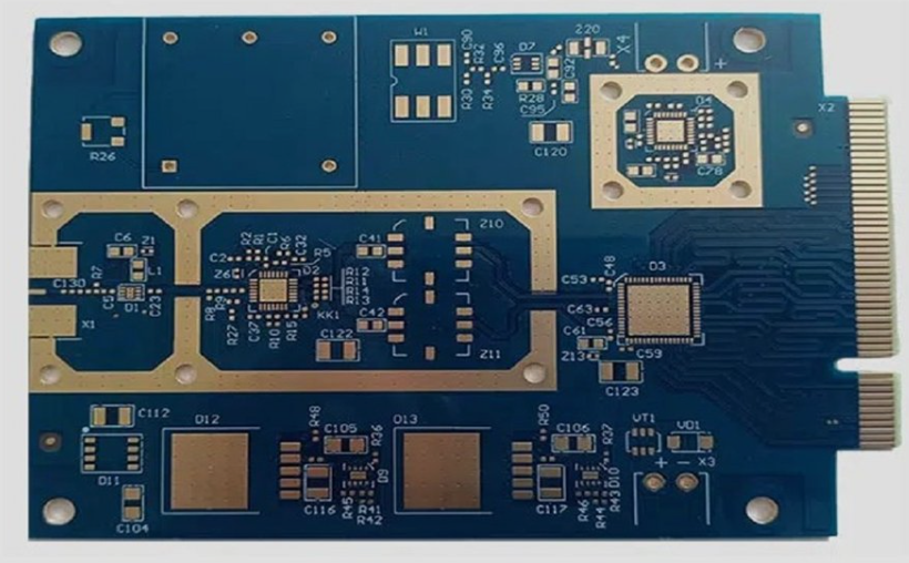
The connector is the point where a well-designed cable meets the product, and the board layout around it determines how much of the shield’s work survives. Bond the connector shell to the chassis or to a low impedance ground plane over a large area rather than with a narrow trace, place transient protection close to the connector so that the discharge current does not travel into the board, and add a common mode choke or a ferrite bead where the interface requires additional attenuation.
Signal routing inside the product should preserve the benefit. Keep the data pair short and matched, avoid routing it parallel to switching nodes or power wiring, and give it a continuous reference plane. Where the interface must pass through a panel, the mechanical bond between the connector and the enclosure is part of the electrical design, and the protection measures described for ESD on board edges and in EMI suppression principles apply at that point. The assembly practice that keeps the shield bond intact through production is covered in PCB cable assembly.
Choosing a Cable for the Application
Not every installation needs the most heavily shielded cable available. The decision should follow from the measured environment: where a drive switches large currents close to the instrument, a double braid over foil with careful shield termination is justified, while a panel with only low power switching may be served by a braid and foil construction. Overspecifying the cable adds cost, diameter and stiffness without improving the result if the termination and the grounding are not correct.
Two construction details are worth checking on any candidate. The first is that the data conductors form a twisted pair with a uniform lay length, since an irregular twist leaves the two conductors unequally exposed and converts part of the disturbance into a differential error. The second is the quality of the bond between the shield and the connector shell: a moulded assembly that provides a continuous circumferential contact is preferable to one where the shield is folded back and soldered to a single point.
Installation Practice in a Cabinet
Two identical instruments can behave differently because of how the cable is installed. Running the USB cable alongside a motor cable for several metres couples the disturbance directly into the shield and the data pair, and the resulting common mode current is often larger than anything generated inside the instrument. Separating the cable from power wiring, crossing other cables at right angles rather than running parallel, and keeping the excess length coiled rather than laid along a drive cable are simple measures with measurable effect.
Where the instrument is mounted in a cabinet with drives, the enclosure itself is part of the shield. A metal cabinet with a bonded door and a properly terminated cable gland presents a much lower impedance environment than a plastic housing, and the connector to chassis bond inside the instrument should be verified with a low resistance measurement rather than assumed from the mechanical assembly.
FAQ
Does a more expensive cable always fix the problem? No. A cable with better shielding and correct termination removes one coupling path, but if the disturbance enters through a ground loop or a poorly bonded connector, the result does not change.
Is a ferrite clamp on the cable a substitute for a proper shield? It is a supplement, not a substitute. A clamp raises the impedance of the common mode path and can resolve a marginal case, but it cannot compensate for a shield that is terminated through a long pigtail.
How can an intermittent fault be confirmed as a shielding issue? Reproduce it with the disturbing equipment running, then measure the shield current and the common mode voltage on the data pair. A fault that tracks the operation of a nearby drive is a coupling problem, not a protocol problem.