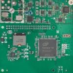
Wearable PCBA: Micro Placement in Small Batch Runs
The difficulty of a wearable PCBA is hidden in the word small. To reduce the size of the product, the design uses 0201 passives, fine pitch QFN devices, miniature connectors and densely packed components, and the pad spacing that results leaves very little margin in printing, placement and reflow. A board that looks simple on a drawing is, in production terms, one of the more demanding assemblies a line will see.
Wearables also move quickly. A prototype becomes a trial batch of a few dozen or a few hundred units, and the design is still being adjusted for power consumption, mechanics or radio performance while that happens. The factory therefore has to do more than solder the boards: it has to notice the mismatches between the data, the material and the process before they become a batch of defects.
Reviewing the Data Before the Build
The enquiry package contains the fabrication data, the bill of materials, the placement coordinates, the assembly drawing, the stencil requirement and the programming and test instructions. Where the product uses a flexible or rigid-flex board, or an unusual panel arrangement, the locating method, the keep-out areas and the component height limit are stated as well.
The bill of materials cannot be a list of generic values. Package, manufacturer, tolerance, voltage rating and the permitted substitution range all belong in it, because sensors, crystals and low power devices in a wearable are sensitive to the exact part fitted: a substitute can raise the standby current, shorten the radio range or shift a measurement.
Confirming the substitution rules before purchasing is what prevents a stop at the line and a batch of rework. A component that can be exchanged without consequence should be marked as such, and a component that cannot be replaced should be marked just as clearly, so that the decision is made by engineering rather than by availability.
Paste Printing for the Smallest Devices
For 0201 and fine pitch parts, too much paste produces bridging and too little produces joints that are incomplete or intermittent. The printing parameters are set from the pad dimensions, the stencil thickness and the aperture design, and the result is checked for offset, slump and blocked apertures.
Where the equipment allows it, solder paste inspection measures the area, the height and the volume of the deposits. This is not a formality: it intercepts a printing fault while the boards are still worth almost nothing, rather than after the devices have been placed and reflowed, when the same fault has to be corrected by hand on every board.
During placement, the nozzle selection, the feeder condition and the polarity of the parts are all watched. Components this small are light, and the tension of the carrier tape, a build-up of static or a worn nozzle can throw a part or move it after it has been placed. For a board being built for the first time, the first article is fitted and confirmed before the run continues, which is the point at which a wrong feeder or a rotated device is still a single board.
Reflow Across Mixed Thermal Mass
A wearable board carries parts that heat quickly and parts that do not. Small passives, a shield can, a connector and a device with a large pad may sit within centimetres of one another, and they do not reach temperature at the same rate. The reflow profile is written for the board as a whole, with the thermal capacity of the parts, the laminate and the solder paste taken into account.
Insufficient heat leaves joints that have not wetted properly; excess heat affects plastic connectors and temperature sensitive devices, and the damage is not always visible at the time. The profile is confirmed on the first article and recorded for the order, so that a repeat run starts from a known condition rather than from a guess.
After reflow, optical inspection covers displacement, missing parts, reversal, tombstoning, bridging and joint appearance. Where a device has joints that cannot be seen — a QFN, for example — the judgement is made from the process record, from sampling by X-ray where it is warranted, and from the functional test, rather than from the visible surface of the board alone.
<img src="https://www.gopcba.com/wp-content/uploads/2025/05/未标题-5.webp" alt="reflow profile verified on a wearable PCBA trial batch” />
What a Small Batch Trial Should Establish
The value of a trial batch is not only the boards it produces. It is the evidence it generates for the volume build, and that evidence is worth collecting deliberately: material losses by part number, the positions that repeatedly need attention, the reasons for rework, the programme version used and the test results.
Where one device repeatedly shifts or solders poorly, the response is to examine the pad design, the stencil aperture and the packaging of that device. Relying on an operator to correct the same position on every board is a decision to build that defect into the volume process.
The functional test for a battery product covers the switch-on current, the standby current, the charging state, the radio link, the sensor readings and the connector behaviour. The supply polarity, the protection circuit and the test voltage are confirmed as well, because a test that damages the board it is checking is a test that has been designed incorrectly.
Working Between Prototype and Volume
Because the design of a wearable often changes between the prototype and the trial batch, the version discipline matters more here than in most assemblies. The fabrication data, the bill of materials, the coordinates and the programme are kept at one revision, and a change to any of them is applied across the set rather than to a single file.
The processes themselves are the familiar ones — SMT assembly, with flexible boards handled as flex PCB assembly, boards that need programming and verification as PCBA testing, the early builds as rapid PCBA prototyping and the criteria behind the inspection under quality management. What changes with a wearable is the tolerance: the same process has to hold to a finer margin, and the data has to be right before the line starts.
Handling and Packaging a Very Small Assembly
A wearable board is thin, light and easily damaged by pressure that a larger board would ignore. Stacking boards, lifting them by a connector or a shield can, or packing them so that the load passes through a tall component produces damage that is later attributed to the assembly process.
Between operations the boards are supported rather than stacked, and they travel in trays that locate them without touching the parts that must not be touched. Where a board carries an exposed sensor aperture or an optical component, that surface is protected specifically, because a scratch on an optical surface is a functional defect rather than a cosmetic one.
The packaging at the end follows the same reasoning. Antistatic material, trays that hold each board by its edges and a carton that protects the whole stack are the usual arrangement; what varies between products is how much of the protection has to be shaped around the specific devices on the board. Where the customer intends to carry out further assembly, the packing method is agreed in advance so that unpacking does not become the most delicate step in the process.
FAQ
Why is a small board harder to assemble than a large one? Because the devices and the pad spacing are smaller, so the same variation in paste volume or placement position consumes a much larger share of the available tolerance.
Why check the paste before placement? Because a printing fault is cheap to correct at that stage and expensive to correct once the parts have been placed and reflowed.
What should a trial batch record? Material losses, the positions that needed attention, the reasons for rework, the programme version and the test results, since these are what the volume build is planned around.