Printed circuit board assembly (PCBA) is one of the most important stages in electronic product manufacturing. It transforms a bare PCB into a functional electronic assembly by mounting and soldering components such as resistors, capacitors, diodes, integrated circuits, connectors, and other electronic devices onto the board.
Although PCB fabrication creates the physical board structure and conductive circuitry, it is the PCB assembly process that populates the board with electronic components and enables it to perform its intended electrical functions.
From consumer electronics and IoT devices to automotive electronics, medical equipment, industrial automation, communications, and aerospace systems, reliable PCB assembly directly influences electrical performance, product stability, manufacturing consistency, and service life.
This guide explains what PCB assembly is, the major PCB assembly processes, the differences between PCB fabrication and PCBA, common assembly technologies, quality-control methods, and how Kingda supports customers from prototype development through production.
What Is PCB Assembly?
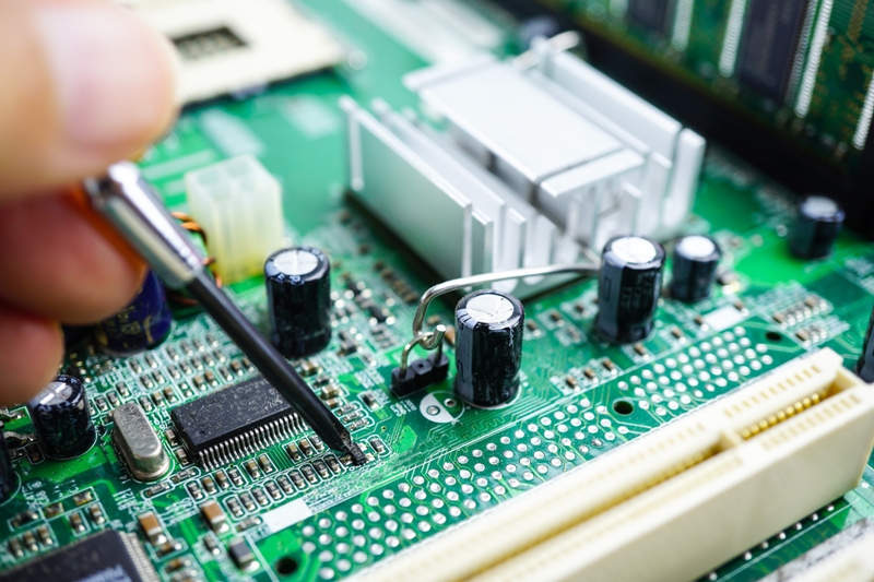
PCB assembly, commonly abbreviated as PCBA (Printed Circuit Board Assembly), is the process of attaching electronic components to a manufactured bare PCB according to an approved circuit design and assembly specification.
The process normally takes place after PCB fabrication has been completed.
A typical PCB assembly process includes:
Solder Paste Printing → Component Placement → Reflow Soldering → THT/PTH Assembly → Inspection → Testing → Final Quality Control → Packaging
Depending on product requirements, additional processes may include:
- Component programming
- Conformal coating
- Dispensing
- Selective soldering
- Functional testing
- Burn-in testing
- Box-build assembly
- Laser marking
- Customized packaging
The final PCBA can then be integrated into the customer’s electronic device or complete product.
PCB Fabrication vs. PCB Assembly
PCB fabrication and PCB assembly are closely related but perform different functions.
| Feature | PCB Fabrication | PCB Assembly |
|---|---|---|
| Main purpose | Manufacture the bare circuit board | Install electronic components |
| Input | Gerber/ODB++/IPC-2581 manufacturing data | Bare PCB + BOM + assembly data |
| Main materials | Copper, laminate, prepreg, solder mask | ICs, resistors, capacitors, connectors, etc. |
| Major processes | Imaging, etching, lamination, drilling, plating | SMT, THT, soldering, inspection, testing |
| Output | Bare PCB | Functional PCBA |
| Components | Not installed | Electronic components installed |
| Functionality | Provides electrical pathways | Performs the designed electronic functions |
In simple terms, PCB fabrication builds the platform, while PCB assembly brings that platform to life.
Why Is PCB Assembly Important?
The quality of the PCB assembly process directly affects the performance and reliability of the final electronic product.
For consumer products, poor soldering can cause intermittent operation or premature failure. For automotive, medical, industrial, or aerospace electronics, assembly defects can have much more serious consequences.
Professional PCB assembly helps ensure:
Reliable Electrical Connections
Correct soldering creates stable electrical connections between components and PCB pads.
Stable High-Speed Performance
Proper component placement, grounding, power distribution, and solder quality are important for high-speed and high-frequency applications.
Thermal Reliability
Correct component placement, soldering profiles, and thermal design help prevent excessive temperature rise and premature component failure.
Long-Term Mechanical Reliability
Reliable solder joints are especially important for products exposed to vibration, shock, temperature cycling, or mechanical stress.
Consistent Mass Production
Automated manufacturing, inspection, and process control allow thousands or millions of boards to be produced consistently.
Types of PCB Assembly
Based on component mounting technology, PCB assembly can generally be divided into three major categories: SMT, THT, and mixed technology.
| Assembly Technology | Component Type | Mounting Method | Typical Soldering | Typical Applications |
|---|---|---|---|---|
| SMT Assembly | Surface-mount devices | Mounted directly on PCB pads | Reflow soldering | Smartphones, IoT, computers, medical electronics |
| THT Assembly | Through-hole components | Leads inserted through PCB holes | Wave/selective/manual soldering | Power electronics, connectors, industrial equipment |
| Mixed Technology Assembly | SMT + THT | Combination | Reflow + wave/selective/manual | Automotive, industrial, communications |
SMT PCB Assembly
SMT (Surface Mount Technology) is the dominant technology used in modern electronic manufacturing.
Instead of inserting component leads through holes, SMT components are placed directly onto copper pads on the PCB surface.
SMT offers several important benefits:
- Higher component density
- Smaller PCB size
- Automated production
- High placement accuracy
- Shorter electrical paths
- Better suitability for high-speed designs
- High production efficiency
Kingda supports high-speed SMT PCB assembly for prototype, low-volume, and larger production programs. Its published capabilities include miniature components, BGA, QFN, QFP, and other fine-pitch packages. (Kingda)
THT / PTH PCB Assembly
THT (Through-Hole Technology), also called PTH assembly, uses components whose leads pass through holes in the PCB.
THT is particularly useful for components that require additional mechanical strength or higher current-carrying capability, including:
- Connectors
- Transformers
- Relays
- Large capacitors
- Power components
- Switches
THT components may be soldered using wave soldering, selective soldering, or manual soldering.
Mixed Technology PCB Assembly
Many modern products require both SMT and THT.
For example, a PCB may use:
- SMT ICs and passive components
- THT connectors
- THT transformers
- Power components
- Mechanical switches
This is known as mixed technology PCB assembly.
Kingda supports integrated SMT and THT manufacturing, including automated placement, reflow, wave soldering, selective soldering, and manual assembly. (Kingda)
PCB Assembly Process: Step by Step
1. Prepare the Manufacturing and Assembly Files
Before production begins, the manufacturer reviews the complete project documentation.
The typical PCB assembly files include:
- Gerber files
- BOM
- Pick-and-Place/Centroid file
- Assembly drawings
- PCB schematic
- Stack-up information
- Testing requirements
- Programming instructions
- Special process requirements
BOM
The Bill of Materials (BOM) contains information about every component required for assembly.
A good BOM should include:
- Reference designator
- Manufacturer
- Manufacturer Part Number (MPN)
- Component description
- Package
- Quantity
- Approved alternatives
- DNP information
Pick-and-Place File
The Pick-and-Place file provides the coordinates and rotation information required by SMT placement machines.
The consistency between the BOM, Gerber files, and Pick-and-Place file is critical. Errors at this stage can lead to incorrect components or incorrect component placement.
2. DFM and DFA Review
Before manufacturing starts, professional PCB assembly manufacturers perform DFM (Design for Manufacturability) and DFA (Design for Assembly) reviews.
The engineering team may check:
- Component-to-component spacing
- Pad dimensions
- Component orientation
- Polarity markings
- PCB edge clearance
- Solder-mask clearance
- Footprint compatibility
- Component availability
- Assembly accessibility
- Potential soldering problems
Kingda provides engineering support including DFM/DFA analysis, BOM verification, Gerber review, Pick-and-Place verification, and manufacturing optimization. (Kingda)
Early engineering review helps identify problems before materials are purchased and production begins.
3. SMT Stencil Preparation
An SMT stencil is used to transfer solder paste onto PCB pads.
The stencil contains precisely manufactured apertures corresponding to the solder pads on the PCB.
Stencil quality affects:
- Solder paste volume
- Solder joint quality
- Fine-pitch assembly performance
- Solder bridging
- Component reliability
For fine-pitch and miniature components, aperture design becomes especially important.
4. Solder Paste Printing
During solder paste printing, the PCB is aligned with the stencil and solder paste is applied using a squeegee.
The paste passes through the stencil openings and forms deposits on the PCB pads.
Important parameters include:
- Stencil thickness
- Aperture dimensions
- Solder paste type
- Printing speed
- Squeegee pressure
- Alignment accuracy
- PCB support
After printing, SPI (Solder Paste Inspection) can measure solder paste volume, height, area, and position.
Kingda lists 3D SPI as part of its PCB assembly inspection capabilities. (Kingda)
5. SMT Component Placement
After solder paste printing, the PCB is transferred to the pick-and-place machine.
The machine automatically places electronic components onto the solder paste according to the approved placement program.
Advanced placement systems use vision recognition to verify:
- PCB fiducials
- Component orientation
- Component position
- Package characteristics
- Placement accuracy
Kingda’s published SMT capabilities include support for miniature passives such as 01005 and 0201, as well as BGA, QFN, QFP, and other fine-pitch components. (Kingda)
6. First Article Inspection
For new projects or production changes, FAI (First Article Inspection) can be used to verify the first assembled board before continuing with the full batch.
Engineers may verify:
- Component identity
- Component orientation
- Placement accuracy
- Soldering quality
- BOM consistency
- Assembly drawing compliance
This step helps prevent a systematic production error from affecting an entire batch.
7. Reflow Soldering
After component placement, the PCB enters the reflow soldering oven.
The board passes through controlled temperature zones, typically consisting of:
Preheat → Soak → Reflow → Cooling
During the reflow stage, the solder paste melts and forms permanent electrical and mechanical connections between the components and PCB pads.
An appropriate thermal profile is essential because excessive temperature can damage sensitive components, while insufficient heating can result in poor solder wetting.
Common reflow defects include:
- Cold solder joints
- Solder bridging
- Tombstoning
- Insufficient solder
- Voiding
- Component damage
Kingda reports the use of multi-zone reflow equipment to control soldering profiles for SMT production. (Kingda)
8. AOI Inspection
After reflow, the board undergoes AOI (Automated Optical Inspection).
AOI uses cameras and image-processing algorithms to identify visible assembly defects such as:
- Missing components
- Incorrect orientation
- Component displacement
- Solder bridges
- Tombstoning
- Incorrect polarity
- Visible solder defects
AOI significantly improves inspection consistency compared with relying solely on manual inspection.
9. X-Ray Inspection
Some solder joints cannot be inspected optically.
This is particularly true for:
- BGA
- QFN
- LGA
- CSP
- Other hidden-pad packages
X-ray inspection allows manufacturers to inspect hidden solder joints and identify:
- Voids
- Open joints
- Insufficient solder
- Bridging
- Misalignment
- Poor solder connections
Kingda lists X-ray inspection as part of its PCB assembly quality-control system. (Kingda)
10. Through-Hole Assembly
After SMT assembly, THT components can be installed where required.
The general process is:
Component Insertion → Position Verification → Wave/Selective Soldering → Lead Cutting → Inspection
Depending on the product, components can be inserted manually or using automated equipment.
11. Wave and Selective Soldering
Wave Soldering
Wave soldering is commonly used for larger-volume THT production.
Molten solder forms a controlled wave that contacts the exposed component leads and PCB pads, creating solder joints simultaneously.
Selective Soldering
Selective soldering is especially useful for mixed SMT/THT boards.
Instead of exposing the entire PCB underside to molten solder, only the selected through-hole locations are soldered.
This can reduce thermal stress and protect nearby SMT components.
Kingda provides wave and selective soldering capabilities for mixed-technology PCB assemblies. (Kingda)
12. Cleaning and Post-Solder Processing
After soldering, the PCB may require cleaning to remove flux residues and contaminants.
The cleaning method depends on:
- Flux type
- Product requirements
- Cleanliness specifications
- Environmental requirements
Additional processes may include:
- Conformal coating
- Dispensing
- Adhesive application
- Shield installation
- Connector installation
- IC programming
For products used in harsh environments, conformal coating can provide additional protection against moisture, dust, and chemical exposure.
13. Electrical and Functional Testing
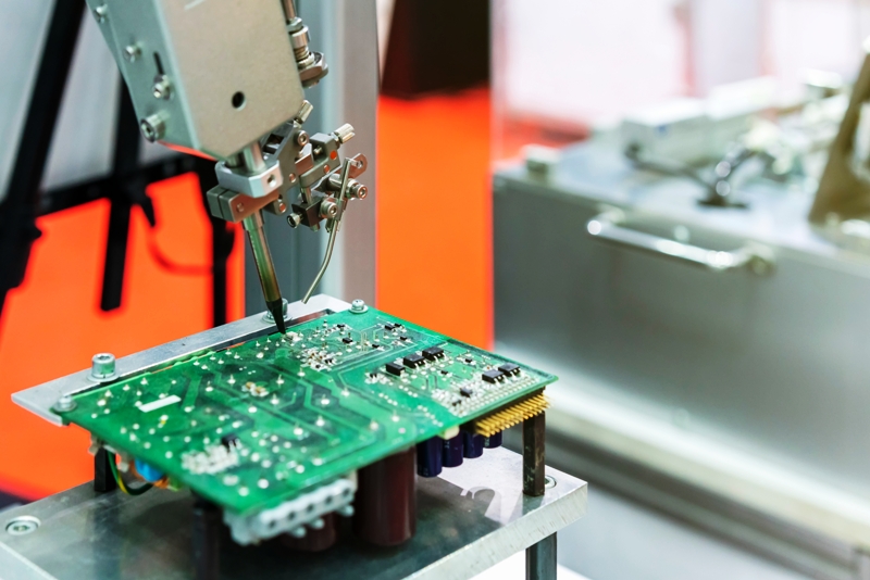
After assembly, PCBA testing verifies whether the board works correctly.
Common testing methods include:
Visual Inspection
Checks components, solder joints, connectors, labels, and board condition.
AOI
Automated inspection for visible assembly defects.
X-Ray
Inspection of hidden solder joints.
ICT
In-Circuit Testing (ICT) checks electrical characteristics and circuit connectivity using a dedicated test fixture.
FCT
Functional Testing (FCT) simulates actual product operation to verify whether the assembled PCB performs its intended functions.
Kingda supports AOI, X-ray, FAI, ICT, FCT, and customized testing solutions according to customer requirements. (Kingda)
14. Final Quality Control
After all production and testing processes are completed, the PCB assembly undergoes final quality control.
The inspection may include:
- Component verification
- Solder quality
- Appearance
- Labeling
- Test results
- Packaging
- Customer-specific requirements
A structured quality system helps ensure consistency from incoming material inspection through final shipment.
Kingda states that its quality-control flow covers IQC → SPI → SMT/THT Assembly → AOI → X-Ray → ICT/FCT → OQC, with traceability maintained throughout production. (Kingda)
15. Labeling and Traceability
Electronic products often require identification and traceability information.
Typical identification methods include:
- Serial numbers
- QR codes
- Barcodes
- Part numbers
- Revision numbers
- Production information
- Customer-specific labels
Traceability makes it easier to manage production records, investigate quality issues, support warranty service, and control product revisions.
Kingda states that its manufacturing records and inspection data are maintained through a traceability system covering the production lifecycle. (Kingda)
16. Packaging and Shipment
The last stage is PCB assembly packaging.
Electronic assemblies need protection against:
- ESD
- Moisture
- Dust
- Mechanical shock
- Vibration
- Transportation damage
Common packaging methods include:
- ESD-safe bags
- Anti-static trays
- Moisture-barrier bags
- Foam protection
- Reinforced cartons
- Customer-specific packaging
Kingda states that completed PCB assemblies are packaged using anti-static and protective materials and supported by global logistics partners for delivery. (Kingda)
PCB Assembly Quality Control
Quality cannot rely on a single inspection method. Different inspection technologies identify different defect types.
A comprehensive PCB assembly quality control system may include:
IQC → SPI → FAI → SMT/THT Assembly → AOI → X-Ray → ICT → FCT → OQC
SPI
Detects solder-paste printing problems before components are placed.
AOI
Detects visible component-placement and soldering defects.
X-Ray
Detects hidden solder-joint defects.
ICT
Checks electrical characteristics and circuit connectivity.
FCT
Verifies actual functional performance.
This layered inspection approach is particularly important for automotive, medical, industrial, communications, and other high-reliability applications.
After Assembly Services
Modern PCB assembly services often extend beyond basic SMT and THT assembly.
Depending on project requirements, value-added services may include:
Conformal Coating
Protects the PCBA from moisture, chemicals, dust, and environmental contamination.
IC Programming
Firmware or software can be programmed into microcontrollers and memory devices before shipment.
Cable and Wire Harness Assembly
Cables and harnesses can be integrated with PCBAs to simplify final product assembly.
Box Build Assembly
Box build assembly integrates the PCBA with:
- Enclosures
- Cable assemblies
- Displays
- Mechanical components
- Power supplies
- Connectors
- User interfaces
Kingda provides one-stop manufacturing that extends from PCB fabrication and component procurement through SMT/DIP assembly, finished-product assembly, testing, and system integration. (Kingda)
Why Choose Kingda for PCB Assembly?
One-Stop PCB and PCBA Manufacturing
Founded in 2013, Kingda describes itself as a one-stop PCBA manufacturing solution provider integrating PCB design and development, PCB manufacturing, component procurement, SMT, DIP, finished-product assembly, and testing. (Kingda)
This integrated workflow reduces the need to coordinate multiple manufacturing suppliers and simplifies project management.
Prototype to Production
Kingda supports PCB assembly from prototypes and low-volume production through volume manufacturing. Its published rapid-prototyping capabilities include rigid, flex, and rigid-flex boards, with prototype, low-volume, and volume-production options. (Kingda)
Advanced SMT Capabilities
Kingda’s published capabilities include:
- 01005 and 0201 components
- BGA
- QFN
- QFP
- Fine-pitch components
- Mixed-technology assembly
- SMT and THT assembly
Its published prototype capability includes BGA down to 0.25 mm pitch and IC assembly precision of approximately ±0.03 mm. (Kingda)
Comprehensive Inspection and Testing
Kingda supports:
- 3D SPI
- AOI
- X-ray
- FAI
- ICT
- FCT
- Customized testing
This multi-stage quality-control approach helps identify defects at different points in the manufacturing process. (Kingda)
Strong Engineering Support
Kingda provides engineering assistance throughout the manufacturing process, including DFM/DFA analysis, BOM validation, Gerber review, component analysis, sourcing, and production optimization. (Kingda)
Quality Management and Certifications
Kingda states that it has obtained ISO 9001, ISO 13485, IATF 16949, ISO 14001, and UL certification, while also following IPC-related assembly and quality requirements. (Kingda)
These quality systems are particularly relevant to applications such as automotive electronics, medical devices, industrial automation, communications, and other demanding electronic products.
Global Manufacturing Support
Kingda reports more than 400 employees and more than 5,000 completed projects on its website, with manufacturing and engineering capabilities designed to support customers in multiple industries worldwide. (Kingda)

Conclusion
Understanding what PCB assembly is is essential for anyone involved in electronic product development and manufacturing.
The PCB assembly process is not simply a matter of placing components onto a board. It is a controlled manufacturing system that includes:
SMT provides the high-density and automated assembly capability required by modern electronics, while THT provides additional mechanical and electrical advantages for specific components. Combining these technologies allows manufacturers to build sophisticated mixed-technology PCB assemblies.
For engineers and product developers, selecting the right PCB assembly manufacturer is as important as the PCB design itself. Engineering support, component sourcing, process control, inspection capabilities, testing, traceability, certifications, and scalability should all be considered.
With its one-stop manufacturing model, Kingda integrates PCB fabrication, component procurement, SMT/DIP assembly, testing, finished-product assembly, and system integration, helping customers move from prototype development to production with a more streamlined and controlled manufacturing workflow. (Kingda)