What Is Quick-Turn PCB Manufacturing?
As electronic products become more advanced and market competition becomes increasingly intense, companies need to develop, test, and launch products faster than ever. Traditional PCB production may take several weeks, which can delay product validation and increase development costs.
To meet the demand for shorter development cycles, PCB manufacturers offer Quick-Turn PCB Manufacturing services. This production method reduces the time required to fabricate and deliver printed circuit boards from several weeks to only a few days. Depending on the board design, material availability, and manufacturing requirements, some standard prototypes may even be completed within 24 hours.
A Quick-Turn PCB is a printed circuit board manufactured and delivered in a shorter period than a standard PCB. These boards are particularly useful for engineering prototypes, design verification, functional testing, and low-volume production.
Quick-turn services combine rapid engineering review, efficient material preparation, optimized manufacturing processes, and accelerated quality inspection. They provide engineers with faster access to physical boards, allowing them to identify design problems, make improvements, and validate products without unnecessary delays.
Kingda provides rapid PCB fabrication services for prototypes, small-batch orders, and selected production projects. Typical lead times depend on board complexity, material requirements, quantity, and testing specifications.
What Are the Benefits of Quick-Turn PCB Manufacturing?
1. Shorter Development Time
The most important advantage of Quick-Turn PCB Manufacturing is reduced development time.
After receiving the PCB design files, the manufacturer can quickly perform an engineering and DFM review. This process helps identify potential problems related to trace spacing, hole sizes, layer stackup, materials, solder mask, impedance, and assembly requirements.
Identifying these issues before production can prevent unnecessary delays and reduce the risk of producing defective boards. Faster prototype delivery also allows engineers to test their designs earlier and make corrections before moving to the next development stage.
2. Lower Overall Development Costs
Quick-turn production can help reduce the total cost of product development.
Although an expedited PCB order may have a higher unit price than a standard order, the shorter lead time can reduce other project costs. For example, engineers can discover design errors earlier, avoid extended debugging periods, and prevent expensive problems during mass production.
Early prototype testing also reduces the risk of investing in a large production run before the design has been fully verified. As a result, rapid PCB fabrication can improve both time efficiency and cost control.
3. Improved Flexibility
Product development rarely follows a completely fixed plan. Engineers may need to change component placement, modify routing, adjust the layer stackup, or replace materials after testing the first prototype.
A PCB Prototype produced through a quick-turn service allows design teams to complete more development iterations within the same project schedule. This flexibility is especially valuable for products with complex functions, new technologies, or strict market deadlines.
4. Better Scalability
Quick-turn services can support more than prototype production. Depending on the supplier’s equipment and process capabilities, they may also be used for pre-production batches and selected production runs.
A reliable supplier should be able to support the transition from a small prototype order to a larger production order while maintaining consistent materials, manufacturing standards, and quality requirements.
5. Faster Time to Market
A shorter PCB Manufacturing Lead Time allows companies to complete product validation and market preparation earlier.
For industries such as telecommunications, automotive electronics, industrial equipment, consumer electronics, and medical devices, faster product introduction can provide a significant competitive advantage.
Applications of Quick-Turn PCBs
The available quick-turn services depend on the manufacturer’s equipment, materials, engineering capabilities, and production capacity. Some suppliers focus only on standard FR-4 boards, while others can manufacture more advanced PCB types.
Common applications include the following.
PCB Prototypes
Quick-turn production is widely used for prototype development. Engineers can obtain physical boards quickly and use them to verify circuit performance, mechanical dimensions, component placement, and assembly compatibility.
Prototype boards can also reveal problems that may not be visible during schematic design or simulation, including:
- Incorrect component footprints
- Routing errors
- Signal-integrity problems
- Thermal issues
- Mechanical interference
- Assembly difficulties
- Manufacturing limitations
Pre-Production Batches
A pre-production batch normally contains more boards than a prototype order. It provides a larger sample size for evaluating manufacturing consistency and product performance.
Pre-production testing can help confirm:
- Process stability
- Assembly yield
- Electrical performance
- Material compatibility
- Reliability
- Production readiness
Quick-turn manufacturing is useful at this stage because it allows engineering teams to identify remaining problems before committing to mass production.
Low-Volume Production
Some products require only a limited number of boards, especially specialized equipment, industrial systems, research instruments, and customized electronic devices.
In these cases, Rapid PCB Fabrication can provide a practical solution for producing small quantities without requiring the long preparation time associated with large-volume manufacturing.
Production Support
Quick-turn services may also be used when a company needs replacement boards, engineering changes, emergency production support, or additional units before a standard production order is completed.
However, production suitability depends on board complexity, material availability, quality requirements, and the manufacturer’s available capacity.
Factors That Affect PCB Manufacturing Lead Time
Although quick-turn services are designed to shorten delivery schedules, several factors can influence the actual production time.
Manufacturing Capability
The manufacturer’s engineering resources, equipment, process control, and production experience directly affect delivery performance.
A capable quick-turn supplier should be able to coordinate engineering review, material preparation, fabrication, inspection, and shipping without unnecessary interruptions.
Equipment and Production Capacity
Modern equipment can improve manufacturing efficiency and reduce processing time. Important equipment includes:
- CNC drilling machines
- Laser drilling systems
- Exposure machines
- Imaging equipment
- Plating lines
- Automated inspection systems
- Electrical testing equipment
- CNC routing machines
Production capacity is also important. A supplier with multiple machines can continue production if one machine requires maintenance or becomes unavailable.
Material Availability
Material procurement is one of the most important factors affecting PCB Manufacturing Lead Time.
Common materials such as standard FR-4 may be available from stock. However, special materials, including high-frequency laminates, high-Tg materials, polyimide, metal-core materials, and unusual copper thicknesses, may require additional procurement time.
Before starting production, the manufacturer should confirm:
- Material type
- Laminate thickness
- Copper thickness
- Dielectric requirements
- Surface finish
- Material availability
- Approved alternatives
Selecting an available material early can significantly improve the speed of a quick-turn project.
PCB Design Complexity
The complexity of the PCB design has a direct impact on production time.
Factors that may increase lead time include:
- High layer counts
- HDI structures
- Blind and buried vias
- Microvias
- Fine lines and small spacing
- Heavy copper
- Special surface finishes
- Complex cavities
- Controlled impedance
- Mixed dielectric materials
- Tight dimensional tolerances
A simple two-layer FR-4 board can usually be manufactured faster than a complex multilayer HDI board.
Engineering Review
Engineering expertise is essential for rapid PCB production. A quick-turn supplier must review the design quickly while still identifying potential manufacturing risks.
The engineering review may cover:
- Gerber files
- Drill files
- Stackup
- Material selection
- Minimum trace width and spacing
- Hole size and aspect ratio
- Copper thickness
- Solder mask clearance
- Surface finish
- Electrical testing
- Assembly requirements
If important engineering decisions are delayed, the entire production schedule may be affected.
Special Processes
Special manufacturing requirements can increase lead time. Examples include:
- Countersunk holes
- Controlled-depth routing
- Selective hard gold
- Peelable solder mask
- Via filling
- VIPPO
- Backdrilling
- Edge plating
- Metal plating
- Special surface finishes
These processes should be clearly specified during the quotation and engineering review stages.
Quality Requirements
Quality standards also affect production time. A board requiring advanced inspection, impedance testing, reliability testing, or IPC Class 3 acceptance may require more time than a standard prototype.
A reliable manufacturer should clarify the inspection requirements before production begins.
Shipping Method
Shipping time must also be included in the total project schedule.
Typical delivery methods include:
- Express courier
- Air freight
- Sea freight
Express shipping is usually the fastest option for prototypes and small orders. The final delivery time depends on the destination, customs clearance, package size, and selected carrier.
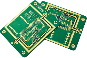
Quick-Turn PCB Manufacturing Process
The typical PCB Production process includes the following stages.
1. PCB Design and File Preparation
The process begins with the PCB design. The customer normally provides Gerber files, drill files, board specifications, stackup information, and other manufacturing documents.
The design files should clearly define:
- Board dimensions
- Layer count
- Material
- Copper thickness
- Minimum trace width
- Minimum spacing
- Hole sizes
- Surface finish
- Solder mask
- Silkscreen
- Electrical testing requirements
Accurate documentation helps prevent engineering questions and production delays.
2. Engineering and DFM Review
The manufacturer checks whether the design can be produced using the available equipment and processes.
The DFM review may identify:
- Insufficient spacing
- Small or unsuitable drill sizes
- Inadequate annular rings
- Unbalanced copper distribution
- Incorrect solder mask openings
- Unclear drill specifications
- Difficult routing structures
- Material or stackup conflicts
Resolving these issues before production is essential for a successful quick-turn order.
3. Material Preparation
After the design is approved, the required laminate, copper foil, prepreg, and other materials are prepared.
The material selection must match the electrical, mechanical, thermal, and reliability requirements of the PCB.
4. Inner-Layer Imaging and Etching
For multilayer boards, the circuit patterns are transferred onto the inner-layer copper using imaging technology.
Unwanted copper is then removed through etching, leaving the required circuit pattern. The inner layers are inspected before lamination.
5. Lamination
For multilayer PCBs, inner layers, copper foil, and prepreg are pressed together under controlled temperature and pressure.
Lamination quality affects:
- Layer registration
- Dielectric thickness
- Board thickness
- Electrical performance
- Mechanical strength
- Reliability
Complex multilayer boards may require additional lamination cycles, which can increase lead time.
6. Drilling
Mechanical or laser drilling is used to create through-holes, blind vias, buried vias, and other required structures.
Small holes, high aspect ratios, and complex via designs require more precise processing and may increase manufacturing time.
7. Copper Plating
Copper plating creates electrical connections between layers and increases the copper thickness on selected surfaces.
Plating quality is important for electrical performance, thermal performance, and long-term reliability.
8. Outer-Layer Imaging and Etching
The outer-layer circuit pattern is transferred, plated, and etched to create the final conductive traces and pads.
The manufacturer must maintain accurate trace width, spacing, registration, and copper thickness during this stage.
9. Solder Mask and Silkscreen
Solder mask is applied to protect exposed copper areas and reduce the risk of solder bridging during assembly.
Silkscreen is used to identify component locations, polarity marks, reference designators, and other assembly information.
10. Surface Finish
Exposed copper pads are protected with a suitable surface finish. Common options include:
- HASL
- Lead-free HASL
- ENIG
- OSP
- Immersion silver
- Immersion tin
- ENEPIG
- Hard gold
The appropriate finish depends on solderability, contact requirements, storage conditions, cost, and application needs.
11. Inspection and Testing
Finished boards undergo inspection and electrical testing to verify compliance with the design.
Possible inspection methods include:
- Automated optical inspection
- Dimensional inspection
- Visual inspection
- Flying probe testing
- Electrical continuity and isolation testing
- Impedance testing
- Microsection analysis
- Reliability testing
For prototypes and small quantities, flying probe testing may be suitable. For larger production volumes, fixture-based testing may provide higher efficiency.
How to Choose a Quick-Turn PCB Supplier
Selecting the right PCB Supplier is essential for achieving both fast delivery and reliable quality.
Delivery Capability
The supplier should provide a clear and realistic lead-time commitment. The quotation should distinguish between manufacturing time and shipping time.
It is also important to confirm whether the stated lead time begins after:
- File approval
- Payment
- Engineering confirmation
- Material confirmation
- Purchase order release
Engineering Support
A reliable supplier should provide professional engineering support before production. Fast communication can prevent misunderstandings and reduce unnecessary design revisions.
The supplier should be able to review:
- PCB design files
- Manufacturing specifications
- Material requirements
- Stackup
- Impedance requirements
- Special processes
- Testing requirements
Manufacturing Equipment
Advanced and well-maintained equipment can improve production efficiency and consistency.
The supplier should have suitable equipment for the required board type, including multilayer fabrication, laser drilling, controlled impedance, special materials, or other advanced processes when necessary.
Quality Management
Speed should never replace quality. A qualified supplier should have a clear quality management system and suitable inspection procedures.
Relevant quality considerations may include:
- IPC requirements
- UL requirements
- Electrical testing
- Dimensional inspection
- Material traceability
- Process control
- Reliability testing
- Final quality inspection
Cost Transparency
The supplier should provide a clear quotation that explains the cost of materials, tooling, testing, special processes, shipping, and other additional services.
A low initial price may not represent the lowest total cost if the supplier cannot meet the required quality or delivery schedule.
Customer Service
Responsive customer service is especially important for quick-turn projects. The supplier should provide timely updates about engineering questions, material availability, production status, inspection results, and shipping.
Why Choose Kingda for Quick-Turn PCB Manufacturing?
Kingda provides Quick-Turn PCB services for prototypes, small-batch orders, and selected production applications. Our engineering and manufacturing teams work closely with customers to reduce unnecessary delays while maintaining product quality.
Kingda’s quick-turn PCB services include:
- Rapid engineering and DFM review
- Prototype and small-batch PCB production
- Multilayer PCB fabrication
- High-Tg and specialized materials
- High-frequency and high-speed PCB options
- Flexible and rigid-flex PCB manufacturing
- HDI and microvia technology
- Controlled-impedance fabrication
- Heavy copper PCB production
- Various surface finishes
- Electrical testing and inspection
- Engineering support throughout the project
Kingda focuses on balancing delivery speed, manufacturing quality, technical capability, and cost efficiency. Before production, our team reviews the design and confirms the material, process, testing, and delivery requirements with the customer.
Conclusion
Quick-Turn PCB Manufacturing is an effective solution for companies that need to shorten product development cycles and obtain circuit boards quickly. It is widely used for prototypes, pre-production testing, low-volume production, and urgent engineering projects.
The actual delivery time depends on many factors, including material availability, board complexity, layer count, via structures, special processes, quality requirements, manufacturing capacity, and shipping method.
To achieve a successful quick-turn project, customers should provide complete design files, select practical materials, confirm manufacturing requirements early, and work with an experienced PCB Supplier.
With professional engineering support, advanced equipment, and strict quality control, Kingda helps customers accelerate PCB Production, reduce development risks, and bring reliable electronic products to market faster.