Wireless Router PCB: A Beginner Guide to Its Design
A wireless router looks like a plastic box with a few antennas, but almost everything that determines whether it works well sits on a single board inside that box. A wireless router PCB has to carry a processor running at hundreds of megahertz, several radio chains operating in the low gigahertz range, a power supply that feeds all of them, and the interfaces that connect to the modem and the local network. Doing all of that without the radios interfering with each other or with the processor is the design problem, and it is a good illustration of why mixed-signal boards are laid out differently from ordinary digital ones.
What the Board Has to Do
The digital side is conventional but demanding. A system-on-chip integrates the processor, the memory controller and the baseband sections, and it runs from a switching supply with several rails that must sequence correctly and stay within tight tolerance. High-speed interfaces between the chip and the memory, and between the chip and the Ethernet magnetics, need controlled impedance and short, direct routing.
The radio side is where the difficulty lies. Each band has its own transmit chain with a power amplifier, its own receive chain with a low noise amplifier, filters and switches, and its own antenna path. Those paths carry signals at power levels spanning many orders of magnitude in the same physical space, so a trace carrying a few milliwatts of received signal may run within a few millimetres of a trace carrying a watt of transmit power. Isolation between them is achieved by distance, by grounded copper between them and by the orientation of the traces, and the layout is judged on how well it does that.
Stack-Up and Layer Planning
Four layers is the practical minimum and six is common in dual-band and tri-band products. The top layer carries components and short routing, the second layer is an uninterrupted ground plane, the third carries power and slow signals, and the bottom layer holds the remaining routing and the ground pour. Putting a solid ground plane immediately beneath the component layer is what makes controlled impedance possible and what gives every fast signal a return path directly underneath it.
Splitting the ground, which is often suggested for mixed-signal boards, is usually a mistake here. The radio sections return their current through the same reference plane as the digital sections, and a plane that is cut into islands forces those return currents to detour, which creates exactly the coupling the split was meant to prevent. Keeping the plane continuous and separating the circuits by placement is the more effective approach, and our layer assignment notes describe how the arrangement is planned.
The RF Front End and Antenna Paths
The RF front end is the group of components between the transceiver and the antenna, and it is the most layout-sensitive part of the board. Transmit and receive paths are usually combined through a switch or a diplexer, and every element between the power amplifier and the antenna contributes loss on transmit and noise figure on receive. Placing those components close together, in the order they appear in the signal chain, keeps the interconnect short and predictable.
Antenna paths deserve special treatment. Where the antenna is external, the path runs to a connector and must be treated as a transmission line for its whole length; where the antenna is printed on the board itself, the feed point, the ground clearance beneath the radiating element and the surrounding copper all become part of the antenna. Removing the ground plane beneath a printed antenna is not optional, and the keep-out extends further than most designers expect. Our design release checklist places the antenna keep-out and the feed checks in the review sequence.
Impedance Control in Practice
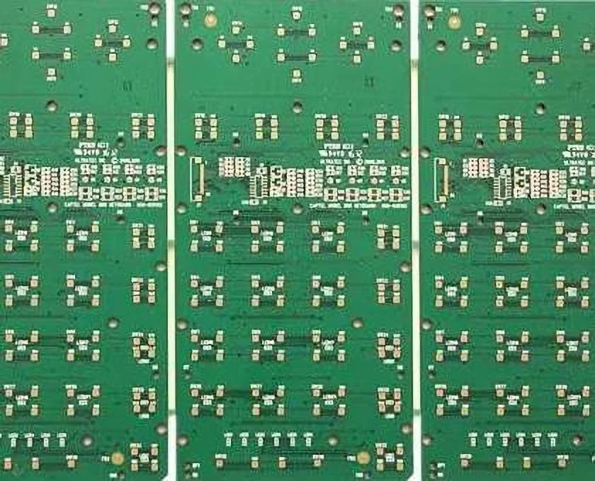
Impedance control means the trace geometry, the dielectric thickness and the reference plane are specified so that the characteristic impedance of the line is a defined value, usually fifty ohms for single-ended radio traces and one hundred ohms differential for the high-speed digital pairs. The fabricator adjusts trace width to hit that value for the stack-up that was quoted, and impedance coupons in the panel border are measured to confirm it.
What breaks impedance control is not the calculation but the layout. A trace that widens to pass around a component, that crosses a plane split, or that runs over a region where the reference plane has been removed for a connector will have a local impedance that differs from the design value, and that discontinuity reflects energy. Keeping radio traces on one layer, avoiding vias in them where possible, and checking that the reference plane is continuous along the whole length are the measures that actually preserve the number the fabricator produced.
Thermal Management in a Sealed Enclosure
A router runs continuously, often in an enclosed cabinet, and its enclosure usually has no fan. The processor and the power amplifiers are the two heat sources that matter, and both conduct most of their heat into the board rather than into the air. Copper under the exposed pad, thermal vias into the internal planes and a generous spreading area on the opposite side are the standard measures, and they work because the copper spreads heat laterally into the whole board area.
The enclosure has to be considered as part of the thermal path. A board that measures acceptably on an open bench can run thirty degrees hotter inside a sealed plastic case, and the derating assumptions for the power amplifier and the regulator should be checked at the internal ambient rather than the room temperature. Our thermal management article describes how that estimate is made before the layout is frozen.
EMI Shielding and Radio Coexistence
Shielding on a router board takes two forms. A metal can soldered over the radio section confines the radiated field and keeps the processor clocks out of the receive path, while local ground stitching and grounded guard traces between sensitive traces keep coupling down without adding components. The stitching vias must be close enough together relative to the highest frequency of interest to prevent the seam between them from acting as a slot.
Coexistence within the board is the harder problem. Two radios transmitting at once can desensitise each other even when each is perfectly designed, and the standard mitigations are physical separation, careful orientation of the antenna paths and a filtering arrangement that keeps the transmit energy of one band out of the receive path of the other. On tri-band products this often drives the decision to place radios on different edges of the board rather than adjacent to one another.
Assembly and Test
The board is assembled with a normal surface mount process, with the shielding cans and the connectors placed on the second pass. Fine pitch components and the dense area around the processor require good stencil design and a placement machine with a vision system, both of which are routine at this density.
Testing is where the radio design is proven. A radio frequency test measures output power, receive sensitivity and spurious emissions on each band across the whole frequency range and at the temperature extremes, and it is normally performed on the finished assembly through a calibrated test port rather than on the bare board. Functional test then covers the network interfaces, the power sequencing and the thermal behaviour under sustained load. If a band fails, the first things to check are the impedance of the antenna path, the ground continuity beneath the radio section and whether the transmit path of another band is leaking into the failing receiver.
FAQ
How many layers does a wireless router PCB need? Four layers is the minimum for a single-band product with a simple antenna, and six layers is typical once two or three bands, Gigabit Ethernet and a dense processor fan-out are combined on one board.
Can the antenna be printed on the same board? Yes, and it is common in compact products, but the antenna then depends on the ground clearance, the surrounding copper and the enclosure, so the keep-out has to be reserved in the layout and honoured through every later revision.
Why does a router get hot when it is idle? The processor clock, the memory and the regulators draw current continuously even when the network is quiet, and the power amplifiers are usually biased to stay ready. That standing dissipation is what the thermal design has to handle, not just the peak transmit condition.