HDI PCB: Structures, Processes and Design Rules for Dense Boards
An HDI PCB, or high-density interconnect board, uses microvias and thin build-up layers to increase the number of connections that fit in a given area. The technology exists because component pitch shrank faster than conventional drilling could follow.
A ball grid array with a thousand balls on a 0.5 mm pitch cannot be escaped with mechanical holes of 0.2 mm and pads large enough to survive the drill tolerance. Microvias solve that problem, and they change the stackup, the fabrication flow and the design rules in the process.
What Defines an HDI Board
The defining feature is the microvia: a hole with a diameter typically below 0.15 mm, formed by laser and plated to connect one layer to the next. A microvia that is drilled through only one dielectric layer is called a single-level microvia; stacked and staggered configurations connect more layers.
HDI boards also use thinner dielectric layers and finer conductor geometry than conventional boards. The combination of small holes, thin dielectrics and fine lines is what raises the achievable routing density.
Build-Up Construction
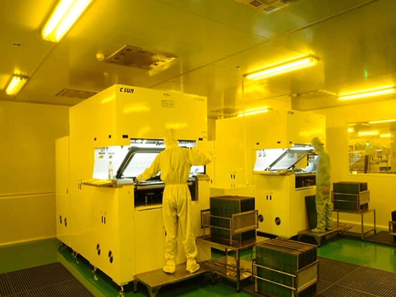
An HDI board is built by sequential lamination. A conventional core is fabricated first, then dielectric layers are added on one or both sides and laser drilled before the next copper layer is plated.
Each build-up cycle adds a pair of layers, or one layer on one side. The type of construction, one, two or three build-up cycles on each side, determines the layer count and the cost, and it is usually described with a notation such as 1+N+1 or 2+N+2.
Because the core is processed with conventional drilling and the build-up layers with laser drilling, the two technologies must be kept compatible. Design rules therefore differ by layer, and the fabrication drawing should state which layers are which.
Microvia Types and Their Reliability
Microvias are classified by how they are stacked. A staggered microvia connects to the layer below with a lateral offset, while a stacked microvia sits directly on top of the one beneath it. Stacked structures save space but concentrate stress at the via base.
Via-in-pad places the microvia directly in the component pad, which allows the pad to be smaller and improves routing. The via must then be filled and plated over so that the pad is flat enough for assembly.
Reliability depends on the plating quality in a very small barrel, on the dielectric material and on the number of thermal cycles the assembly sees. IPC standards define test methods, and the supplier should be able to describe how the microvia will be qualified.
Laser Drilling
Laser drilling is used because mechanical bits at that diameter are impractical and would damage the thin dielectric. The laser energy is absorbed by the copper below the dielectric, so the process is self-limiting when the correct parameters are used.
Conformal masks and copper surface condition affect the result. A dielectric layer that is too thick for the laser energy will not clear completely, leaving a residue that plating cannot cover, which becomes a high-resistance or open connection.
Aspect Ratio Limits
Aspect ratio, the ratio of depth to diameter, limits every drilled and plated hole. For microvias, the practical limit is much lower than for conventional holes, typically around 0.75 to 1, because the plating chemistry must reach the bottom of a very small feature.
Design rules follow directly. Microvias must be drilled through one thin dielectric layer, and connecting several layers requires either stacked or staggered structures rather than a single deep hole.
Design Rules for HDI Layout
Confirm the build-up structure before routing. The number of build-up layers, the layers accessible from each side and the permitted microvia types all determine what routing is legal, and a layout built for a different structure cannot be fabricated.
Keep via-in-pad filled and plated flat. A dimple that exceeds the tolerance leaves a void under the component, and a protruding via prevents the part from seating, which produces opens on every joint of that package.
Manage the copper balance on build-up layers. They are thin, and uneven copper distribution causes lamination stress and registration error, which show up as yield loss rather than as a design error.
Cost Structure
HDI costs more than a conventional board of the same size because the process has more steps. Each build-up cycle adds lamination, laser drilling, plating and inspection, and each one has its own yield.
Cost rises with the number of sequential laminations, the number of microvias, the use of stacked structures and the pitch of the escape required. Where the design can be routed with fewer build-up cycles, the saving is significant.
Escape Routing and Via Selection
Escape routing is the first layout task on a dense package. Each row of a ball grid array must reach a routing channel, and the number of rows that can escape on one layer determines how many build-up layers are needed.
A common sequence is to escape the outer rows on the top layer, place microvias for the inner rows, and continue on the next layer down. Where the pitch is very tight, via-in-pad frees the space that a conventional via fan-out would consume.
The choice between staggered and stacked microvias is made here. Staggered vias need lateral space but distribute stress, while stacked vias save the space and concentrate it. The decision should follow the supplier qualification rather than the layout convenience.
Materials and Electrical Performance
Build-up dielectrics are not the same material as the core. They are formulated for laser drilling, thin lamination and low flow, and their dielectric constant and loss determine the impedance and attenuation of the conductors on those layers.
For high-speed designs, the dielectric thickness of each build-up layer matters to the impedance calculation. Because those layers are thin, traces on them require narrow widths to hold a target impedance, which is one reason fine lines and HDI technology appear together.
Thermal performance also changes. A thin build-up layer conducts heat less effectively than a copper plane, so heat spreading in an HDI board relies on the core and on thermal vias rather than on the surface layers.
Inspection and Yield
Microvias cannot be inspected optically from the outside, so the process relies on coupons, microsections and electrical test. Suppliers include microvia coupons on the panel to verify plating thickness and via integrity.
Yield falls with each build-up cycle, because a defect created in an early cycle cannot be repaired and rejects the whole panel at the end. This is why sequential lamination cost grows faster than the layer count suggests.
When HDI Is Necessary
HDI becomes necessary when the device pitch cannot be escaped on a conventional board, when the component count per unit area exceeds what standard routing allows, or when the electrical performance requires short connections with well-controlled impedance.
It is not automatically necessary for a dense board. A well-planned conventional layout sometimes absorbs the routing without any build-up layers, and that comparison should be made before committing to the more expensive structure.
Related reading: via design rules, electroplating and via filling in HDI, and blind and buried via stack selection.
FAQ
How small can a microvia be? Diameters between 0.075 mm and 0.15 mm are common. The limit is set by laser capability and by the aspect ratio the plating process can fill reliably.
Can HDI vias be stacked? Yes, and stacking saves space, but it also concentrates mechanical and thermal stress. The supplier should confirm that its process and qualification data support the stacking the layout requires.
Is via-in-pad always required with HDI? It is common because it saves pad area, but it requires filling and planarization. Where the design allows an offset via, the process is simpler and less expensive.