10-Layer PCB1.6mm Controlled Impedance PCB for High-Speed Electronics
As a critical platform for modern electronic systems, PCBs face increasingly demanding requirements for signal integrity, routing density, electrical stability, and manufacturing precision. A 10-Layer PCB with a standard 1.6mm finished thickness combines multilayer routing capacity with controlled electrical characteristics, making it suitable for complex high-speed electronic applications.
With ten conductive layers, engineers can allocate dedicated signal, power, and ground layers according to the system architecture. The 1.6mm construction also provides a practical balance between mechanical rigidity, component density, and electrical performance.
For advanced applications, the final stack-up should be determined according to the target impedance, signal speed, copper thickness, dielectric properties, routing density, and manufacturing capabilities rather than relying only on nominal board thickness.
Core Parameters: Precision for Stable Performance
Layer Count and Board Thickness
The ten-layer structure provides substantial space for signal routing, power distribution, ground planes, and functional circuit separation. A 1.6mm finished thickness is widely used in electronic assemblies and can provide a practical balance between mechanical strength and PCB integration requirements.
In communication equipment, for example, a 10-layer 1.6mm board can accommodate high-density components while providing sufficient layer resources for power distribution and high-speed signal routing.
A properly engineered Multilayer PCB stack-up should maintain a predictable relationship between signal layers and their reference planes. This is particularly important when controlled impedance is required.
For additional information about multilayer structures and manufacturing, see Multilayer PCB Manufacturing.
Trace Width and Spacing
Minimum trace width and spacing can reach 3/3 mil in suitable manufacturing conditions. Fine-line routing increases routing density and provides designers with greater flexibility when working with high-speed interfaces and compact electronic assemblies.
For 5G communication equipment, high-frequency signal paths require carefully controlled geometry to minimize discontinuities and unwanted coupling. However, trace width and spacing should always be calculated according to the actual stack-up, copper thickness, dielectric characteristics, and impedance target.
Fine-line fabrication therefore requires close control of imaging, etching, registration, and inspection processes.
Controlled Impedance
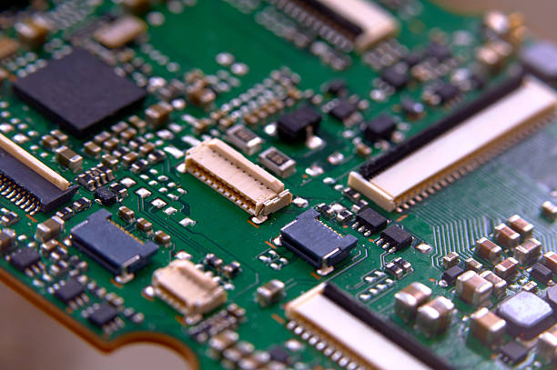
Controlled impedance is one of the defining characteristics of this type of board. Typical impedance tolerances may be specified at ±10%, while more demanding designs can require tighter tolerances depending on the application and manufacturing process.
In high-speed digital circuits, accurate impedance matching helps reduce signal reflection and distortion while supporting stable signal transmission. Applications such as servers, networking equipment, optical modules, and high-speed data interfaces rely on predictable transmission-line characteristics.
Impedance is not determined by trace width alone. Trace geometry, copper thickness, dielectric thickness, dielectric constant, and reference-plane distance all influence the final result.
For a deeper look at differential-pair routing and impedance design, see PCB Impedance Routing and Differential Pair Design.
Small-Diameter Vias
Advanced 10-layer designs may incorporate 0.15mm mechanical blind vias and laser microvias as required by the layout. Smaller interconnection structures can improve routing flexibility and allow designers to escape high-density component packages more efficiently.
Microvia technology is particularly useful around fine-pitch components and high-density interconnect regions. However, via diameter, aspect ratio, pad size, copper thickness, and reliability requirements must be evaluated together during PCB engineering.
For high-density multilayer designs, via structures can also influence signal integrity. Unnecessary via transitions may introduce parasitic effects and impedance discontinuities, making via planning an important part of high-speed PCB design.
Surface Finish
ENIG and other suitable surface finishes can provide reliable solderability, corrosion resistance, and stable electrical contact for many electronic applications.
The appropriate surface finish should be selected according to assembly requirements, contact conditions, environmental exposure, component requirements, and applicable specifications.
For demanding electronic products, surface finishing is only one part of overall PCB reliability. Copper thickness, solder mask quality, plating integrity, dimensional accuracy, and electrical testing must also be controlled.
Advanced Manufacturing Technologies
Laser Drilling Technology
Laser drilling enables the fabrication of small microvias required by high-density multilayer designs. By creating compact interconnection structures, laser drilling can free additional routing space and simplify connections between selected PCB layers.
In RF and high-speed communication equipment, carefully designed microvias can also help reduce unnecessary interconnection structures in critical signal paths.
The quality of laser drilling depends on material properties, laser parameters, target depth, aperture size, positioning accuracy, and subsequent metallization. Consistent process control is essential for reliable microvia formation.
Hybrid Lamination Process
For a ten-layer PCB, precise alignment between copper foil, prepreg, and inner-layer circuits is essential. Lamination must maintain stable layer registration while providing adequate resin flow and interlayer bonding.
Controlled temperature, pressure, heating rate, pressing time, and cooling conditions help reduce defects such as voids, delamination, resin starvation, and excessive board warpage.
For high-speed designs, lamination also directly influences dielectric thickness and therefore affects impedance. Even relatively small variations in dielectric spacing can change transmission-line characteristics.
More information about the relationship between lamination, stack-up, and impedance can be found in High-Speed PCB Lamination and Impedance Control.
3D Impedance Modeling and Simulation
Advanced impedance-controlled boards can benefit from three-dimensional electromagnetic modeling and simulation before fabrication. Simulation allows engineers to evaluate transmission-line geometry, layer transitions, vias, reference planes, and other factors that may influence signal integrity.
Trace width and dielectric thickness can be adjusted during the engineering stage to compensate for expected manufacturing variation.
This approach is particularly useful for high-speed computing and communication systems where small changes in transmission-line geometry can influence signal quality.
The final impedance target should be verified against the actual material stack-up and manufacturing capability. Material dielectric properties should be based on appropriate manufacturer data rather than relying on a generic dielectric constant.
AOI and Electrical Testing
Automated Optical Inspection (AOI) can identify manufacturing defects such as opens, shorts, pattern deviations, missing features, and other circuit abnormalities.
Electrical testing provides an additional level of verification by checking circuit continuity and isolation. For controlled-impedance applications, dedicated impedance test coupons and TDR measurements can be used to verify whether the fabricated transmission lines meet the specified impedance range.
For advanced multilayer boards, combining optical inspection, electrical testing, dimensional inspection, and cross-sectional analysis provides a more comprehensive quality-control process.
Applications Across Advanced Electronics
Communication Equipment
5G Millimeter-Wave Antennas
5G millimeter-wave systems place demanding requirements on PCB materials, routing geometry, impedance control, and signal integrity. A controlled-impedance multilayer structure can provide dedicated signal and reference layers for high-frequency transmission.
High routing density is also valuable for antenna arrays and RF modules where numerous electrical connections must be integrated within a compact footprint.
For RF and microwave applications, material selection becomes especially important because dielectric loss and conductor loss can significantly affect high-frequency transmission performance.
Optical Modules
As communication speeds continue to increase, optical modules require increasingly precise electrical interconnections. High-speed signals such as 112G PAM4 demand carefully controlled transmission paths, appropriate reference planes, and stable impedance.
A ten-layer structure can provide separate power and signal-routing regions while helping reduce unwanted coupling between functional circuits.
Thermal design is also important because high-speed optical modules may generate substantial heat during continuous operation. Copper distribution, component placement, thermal vias, and external cooling structures should therefore be considered together.
For high-speed server and networking applications, High-Speed PCB Prototyping provides additional information about stack-up engineering, material selection, impedance control, and verification.
Automotive Electronics
Autonomous Driving Domain Controllers
Autonomous driving systems process data from cameras, radar, LiDAR, sensors, processors, and communication interfaces. These systems require high-density routing, reliable power distribution, and stable high-speed signal transmission.
A 10-layer 1.6mm controlled-impedance PCB can provide sufficient routing resources for complex electronic control units while allowing engineers to separate high-speed signals, power networks, and reference planes.
However, compliance with automotive functional-safety requirements depends on the complete electronic system and its development process. PCB design and manufacturing should therefore be coordinated with the applicable automotive reliability and validation requirements.
In demanding automotive radar applications, high-frequency PCB technology can provide the material and stack-up options needed for RF signal transmission. High-Frequency PCB Manufacturing covers high-frequency materials, multilayer structures, controlled impedance, fine-line routing, and RF PCB manufacturing considerations.
Medical Imaging
CT Detector Boards
CT detector boards process large numbers of sensitive electrical signals, making signal integrity and noise control particularly important.
A multilayer architecture allows engineers to separate sensitive analog signals from power-distribution and digital circuits while providing strategically positioned ground and reference planes.
Controlled impedance can help maintain predictable transmission characteristics for high-speed signal paths. At the same time, careful grounding, shielding, component placement, and return-current management are required to minimize unwanted interference.
For medical electronics, PCB reliability must be evaluated across electrical performance, manufacturing consistency, environmental conditions, assembly quality, and applicable product-level requirements.
Conclusion
A 10-layer 1.6mm controlled-impedance board combines high routing density, multilayer signal management, compact interconnection structures, and carefully engineered electrical characteristics. These capabilities make it suitable for advanced communication equipment, optical modules, automotive electronics, medical imaging systems, computing platforms, and other high-speed applications.
Successful manufacturing depends on much more than achieving a nominal layer count and board thickness. Stack-up design, trace geometry, dielectric properties, copper thickness, impedance calculation, laser drilling, lamination, registration, surface finishing, AOI, and electrical testing must work together as an integrated manufacturing process.
As electronic systems continue to move toward higher data rates and greater functional density, the combination of 10-Layer PCB, 1.6mm PCB, Controlled Impedance PCB, High-Speed PCB, and Multilayer PCB technologies will remain important for achieving stable signal transmission and reliable electronic performance.