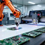
As electronic products continue to deliver higher data rates, faster processing, and greater functional density, high-speed PCB technology has become essential for modern electronics. Applications such as 5G communication, AI servers, data centers, automotive radar, high-performance computing, networking equipment, and advanced industrial systems increasingly depend on high-speed circuit boards to transfer signals accurately and efficiently.
However, achieving reliable high-speed performance is not only a matter of PCB layout. The physical manufacturing process also has a major impact on signal integrity, impedance control, electrical loss, and long-term reliability.
Among all manufacturing stages, PCB lamination is particularly important because it determines the final relationship between copper layers, dielectric materials, and reference planes. Small variations in dielectric thickness, resin distribution, layer registration, or material characteristics can change the electrical behavior of high-speed transmission lines.
Therefore, high-speed PCB lamination requires close coordination between PCB designers, material engineers, and manufacturers.
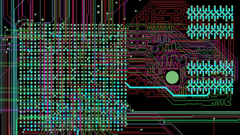
This guide explains the major considerations in high-speed PCB manufacturing, including material selection, stack-up design, impedance control, sequential lamination, vacuum lamination, and post-lamination quality inspection.
What Is PCB Lamination?
PCB lamination is the process of bonding multiple PCB layers into a single rigid structure using controlled heat and pressure.
A typical multilayer PCB contains:
- Copper foil
- Copper-clad laminate
- Prepreg
- Signal layers
- Ground planes
- Power planes
- Dielectric layers
During lamination, these materials are accurately aligned and placed into a controlled press cycle. The resin in the prepreg softens, flows between the layers, and then cures to create a mechanically stable and electrically insulated multilayer board.
For standard PCBs, lamination mainly provides structural integrity. For high-speed PCBs, however, lamination also determines critical electrical characteristics.
The final lamination structure directly affects:
- Characteristic impedance
- Signal propagation speed
- Signal attenuation
- Crosstalk
- Return-path continuity
- Differential-pair balance
- Electromagnetic compatibility
As a result, high-speed PCB lamination must be controlled with significantly greater precision than conventional multilayer PCB production.
Why PCB Lamination Matters for High-Speed Designs
At low frequencies, a PCB trace can often be treated as a simple conductor.
As signal rise time becomes shorter, however, the electrical length of the trace becomes significant. The trace begins to behave as a transmission line, and its physical geometry becomes directly related to electrical performance.
This means that small manufacturing variations can affect system behavior.
For example, a change in dielectric thickness between a signal trace and its reference plane can modify the characteristic impedance. This may result in:
- Signal reflections
- Timing errors
- Increased jitter
- Eye-diagram degradation
- Differential skew
- Crosstalk
- Reduced communication margin
Therefore, PCB lamination for high-speed applications must maintain stable dielectric thickness, reliable resin distribution, and precise layer registration throughout the entire manufacturing panel.
Signal Integrity in High-Speed PCB Lamination
Signal integrity refers to the ability of a signal to travel from one point to another without excessive distortion, attenuation, reflection, or interference.
For high-speed circuits, lamination affects several important signal-integrity parameters.
Dielectric Constant Stability
The dielectric constant, or Dk, influences electromagnetic wave propagation through the PCB material.
If Dk varies significantly across the board, different signal paths may experience different propagation velocities.
This becomes especially important for:
- High-speed differential pairs
- Memory interfaces
- PCIe
- USB
- Ethernet
- RF circuits
- High-speed backplanes
Stable and predictable dielectric characteristics help improve the correlation between simulation results and the final manufactured PCB.
Fiber-Weave Effect
Many PCB laminates use woven fiberglass reinforcement. The dielectric properties of fiberglass bundles differ from those of the surrounding resin.
When high-speed traces are routed directly along specific fiberglass structures, differential signals can experience different propagation environments.
This phenomenon is known as the fiber-weave effect.
Potential consequences include:
- Differential skew
- Phase imbalance
- Timing variation
- Mode conversion
- Reduced signal margin
Engineers can reduce these effects through appropriate routing angles, spread-glass materials, optimized stack-up selection, and careful differential-pair placement.
Impedance Control Through PCB Lamination
Controlled impedance PCB technology is a fundamental requirement for many high-speed interfaces.
Common impedance targets may include:
- 50 Ω for single-ended transmission lines
- 90 Ω for selected differential interfaces
- 100 Ω for many high-speed differential interfaces
The exact value depends on the interface and system architecture.
Impedance is determined by several physical parameters:
- Trace width
- Trace thickness
- Dielectric thickness
- Dielectric constant
- Reference-plane distance
- Copper geometry
This is why high-speed PCB lamination has a direct effect on impedance.
For example, if the dielectric layer is compressed during lamination, the distance between a signal layer and reference plane changes. Even when the original trace width remains unchanged, the impedance can shift.
Manufacturers therefore need to carefully control:
- Prepreg selection
- Resin content
- Lamination pressure
- Lamination temperature
- Press cycle
- Final dielectric thickness
- Copper thickness
For controlled-impedance boards, TDR impedance testing and impedance coupons can be used to verify that manufactured boards meet the specified impedance range.
Key High-Speed PCB Lamination Techniques
1. Sequential Lamination
Sequential lamination is widely used for complex multilayer and HDI PCB structures.
Instead of bonding all layers in a single pressing cycle, sections of the board are fabricated and laminated in multiple stages.
This approach supports advanced structures such as:
- Blind vias
- Buried vias
- Microvias
- Stacked microvias
- HDI build-up layers
- High-density BGA breakout structures
Sequential lamination provides increased routing flexibility and enables compact designs, but it also introduces additional manufacturing complexity.
The process requires precise control of:
- Layer registration
- Lamination thickness
- Thermal stress
- Via alignment
- Resin flow
Therefore, engineers should confirm the manufacturer’s sequential lamination capabilities before finalizing the PCB architecture.
2. Vacuum Lamination
Vacuum PCB lamination removes trapped air from the lamination chamber and promotes more uniform pressure across the PCB stack.
The major benefits include:
- Improved resin flow
- Reduced void formation
- Better interlayer bonding
- More uniform dielectric distribution
- Improved long-term reliability
For advanced multilayer and high-speed PCBs, vacuum-assisted lamination can help maintain consistent structural and electrical characteristics.
3. Controlled Heating and Cooling
Temperature control is another important part of PCB lamination manufacturing.
Excessively rapid heating may cause:
- Uneven resin flow
- Material stress
- Lamination defects
Rapid cooling can increase:
- Warpage
- Internal stress
- Layer movement
- Delamination risk
A controlled heating and cooling profile helps maintain dimensional stability and reduces stress within the finished PCB.
High-Speed PCB Stack-Up Design
The PCB stack-up provides the physical foundation for high-speed signal transmission.
A well-designed stack-up should provide:
- Continuous reference planes
- Controlled dielectric spacing
- Stable impedance
- Efficient power distribution
- Low-noise return paths
- Balanced mechanical construction
For example, a six-layer high-speed PCB could use a structure such as:
| Layer | Function |
|---|---|
| L1 | High-speed signal |
| L2 | Ground plane |
| L3 | Signal |
| L4 | Power |
| L5 | Ground plane |
| L6 | High-speed signal |
The actual stack-up must be customized according to:
- Signal-speed requirements
- Impedance targets
- Number of power domains
- Component density
- Thermal requirements
- Manufacturing capabilities
A symmetrical stack-up is generally preferred because it helps reduce mechanical deformation during pressing and cooling.
Dielectric Thickness and High-Speed Performance
The dielectric thickness between a signal layer and its reference plane has a strong influence on impedance and coupling.
In many high-speed PCB designs, thinner dielectric structures are used to improve coupling between the signal and reference plane.
However, thinner dielectric layers are also more sensitive to manufacturing variation.
For example, a small absolute thickness deviation can represent a relatively large percentage variation when the dielectric layer is extremely thin.
Therefore, achieving stable impedance requires tight control of post-lamination dielectric thickness rather than relying only on theoretical calculations.
Selecting Materials for High-Speed PCB Manufacturing
Material selection is one of the most important steps in high-frequency PCB manufacturing.
Dielectric Constant — Dk
Dk affects propagation velocity and impedance.
A stable Dk helps engineers achieve predictable electrical performance across the board.
Dissipation Factor — Df
Df indicates dielectric loss.
Lower Df materials are generally preferred for demanding high-speed and high-frequency applications because they help reduce signal attenuation.
Thermal Stability
Material characteristics such as:
- Tg
- CTE
- Thermal decomposition temperature
- Moisture absorption
- Dimensional stability
should also be evaluated when selecting laminates.
Material Categories
Depending on performance requirements, common material options include:
- Standard FR-4
- Enhanced FR-4
- Mid-loss laminates
- Low-loss laminates
- Hydrocarbon-based laminates
- PTFE-based materials
- Ceramic-filled materials
- Hybrid material stack-ups
The objective is to find the correct balance between:
Electrical performance + thermal reliability + manufacturability + availability + cost
Using the most expensive laminate is not always the best engineering solution. Material selection should be based on the actual frequency, data rate, channel length, environmental requirements, and production volume.
Manufacturing Considerations for High-Speed PCB Lamination
Even an excellent PCB layout can fail when the manufacturing process cannot reproduce the intended physical structure consistently.
Layer Registration
High-density and high-speed boards require precise layer alignment.
Registration errors can alter:
- Trace geometry
- Signal-to-plane spacing
- Differential-pair symmetry
- Via positioning
- Controlled impedance
Modern high-speed PCB manufacturers therefore use optical alignment, X-ray registration, and other inspection technologies to control layer positioning.
Resin Flow
During lamination, prepreg resin needs to flow evenly around copper patterns.
Incorrect resin flow can result in:
- Voids
- Resin starvation
- Uneven dielectric thickness
- Local mechanical weakness
- Delamination
Manufacturers must therefore control:
- Prepreg resin content
- Copper pattern density
- Lamination pressure
- Heating profile
- Cooling profile
Copper Balance
Large differences in copper distribution across a PCB panel can affect resin flow and thermal expansion.
Copper balancing can help reduce:
- Board warpage
- Uneven resin distribution
- Lamination stress
- Dimensional instability
This is especially important for large multilayer and high-density circuit boards.
Post-Lamination Testing and Inspection
Quality verification should not stop when the lamination press cycle is finished.
Cross-Section Analysis
Microsection or cross-section analysis can verify:
- Layer alignment
- Dielectric thickness
- Copper thickness
- Via structure
- Plating quality
- Lamination bonding
This provides direct evidence of whether the manufactured structure matches the design specification.
TDR Impedance Testing
TDR impedance testing can measure the actual impedance characteristics of controlled-impedance structures.
For example:
Target Impedance: 50 Ω ± 5%
Test coupons manufactured alongside the PCB can provide valuable production data and help correlate physical measurements with simulation models.

Dimensional Inspection
Manufacturers may also inspect:
- Finished board thickness
- Panel dimensions
- Hole locations
- Warpage
- Layer registration
- Board outline
These measurements help prevent issues during PCB assembly and final product integration.
Common High-Speed PCB Lamination Problems and Solutions
Delamination
Delamination occurs when PCB layers fail to bond correctly.
Possible causes include:
- Incompatible materials
- Poor surface treatment
- Excessive moisture
- Incorrect press parameters
- Excessive thermal stress
Preventive measures include proper material matching, moisture control, validated lamination cycles, and adequate surface preparation.
Signal Skew
Signal skew may result from unequal signal propagation paths or differences in local dielectric environments.
The fiber-weave effect is one potential contributor.
Possible solutions include:
- Spread-glass materials
- Controlled routing angles
- Optimized stack-up design
- Better differential-pair routing strategies
PCB Warpage
Warpage is commonly associated with:
- Asymmetric stack-ups
- Uneven copper distribution
- Improper cooling
- Uneven resin flow
- Thermal stress
A symmetrical stack-up and controlled lamination process can significantly reduce warpage risk.
Impedance Variation
PCB impedance variation can result from:
- Dielectric thickness variation
- Trace-width variation
- Copper-thickness variation
- Dk inconsistency
- Etching variation
- Layer-registration problems
This is why high-speed PCB design and manufacturing should be treated as a coordinated engineering process rather than two independent activities.
High-Speed PCB Lamination Process Flow
The complete process can be summarized as:
Material Selection → Stack-Up Engineering → Inner-Layer Fabrication → Surface Treatment → Layer Alignment → Prepreg Lay-Up → Vacuum Lamination → Controlled Cooling → Dimensional Inspection → Mechanical/Laser Drilling → Desmear → Copper Plating → Outer-Layer Fabrication → Surface Finish → Impedance Testing → Final Inspection
This integrated process ensures that the physical PCB structure accurately reflects the electrical assumptions used during design.
How to Improve High-Speed PCB Lamination Results
Involve the Manufacturer Early
Do not finalize a high-speed stack-up solely based on generic impedance calculators.
A manufacturer can provide practical recommendations based on:
- Available laminates
- Prepreg combinations
- Press capabilities
- Copper thickness
- Minimum feature sizes
- Production volume
Define Impedance Requirements Clearly
The manufacturing documentation should specify:
- Single-ended impedance
- Differential impedance
- Target tolerance
- Layer location
- Trace geometry
- Test coupon requirements
Confirm Material Availability
The best technical material is not always the best manufacturing material.
A laminate that is readily available for a prototype may become expensive or difficult to source for volume production.
Validate Prototype-to-Production Compatibility
Whenever possible, use a material and stack-up strategy that can remain stable as the project moves from:
Prototype → Engineering Validation → Pilot Production → Mass Production
This helps reduce redesign risks caused by material substitutions.
Request Production Test Data
For controlled-impedance designs, ask for:
- TDR results
- Test coupon data
- Cross-section reports
- Thickness measurements
- Registration data
These provide objective evidence that the manufacturing process matches the engineering specification.
Why Choose Kingda for High-Speed PCB Manufacturing?
Kingda provides integrated PCB manufacturing and PCBA services for customers developing high-performance electronic products.
Engineering and DFM Support
Kingda can provide engineering support covering:
- Stack-up review
- Impedance analysis
- DFM review
- Gerber verification
- Material selection
- Manufacturing process evaluation
- BOM review
- Production optimization
Early engineering collaboration helps identify potential manufacturing problems before they affect production schedules.
Advanced PCB Manufacturing Capabilities
Kingda supports demanding PCB structures including:
- High-speed multilayer PCBs
- HDI PCBs
- Rigid PCBs
- Flexible PCBs
- Rigid-flex PCBs
- Fine-line PCBs
- High-density interconnect structures
Projects can be developed from prototype through volume production with a consistent manufacturing strategy.
Integrated PCB and PCBA Services
Kingda’s one-stop manufacturing model can integrate:
PCB Fabrication → Component Sourcing → SMT Assembly → THT Assembly → AOI → SPI → X-Ray → ICT/FCT → Conformal Coating → Box Build
This reduces the need to coordinate multiple suppliers and helps improve manufacturing consistency.
Component Procurement and Supply Chain Support
High-speed boards often depend on specialized processors, memory devices, connectors, power ICs, and other advanced components.
Kingda supports:
- BOM verification
- Component sourcing
- Approved alternatives
- Lifecycle analysis
- Supply-chain risk assessment
- Procurement coordination
Prototype to Mass Production
Kingda can support customers through different manufacturing stages:
Rapid Prototype → Low-Volume Production → Pilot Production → High-Volume Manufacturing
Maintaining manufacturing continuity across these stages helps preserve engineering knowledge and reduces transfer risks.
High-Speed PCB Lamination Checklist
Before production, engineers should confirm the following:
Materials
- Laminate family
- Dk
- Df
- Tg
- CTE
- Moisture resistance
- Copper roughness
Stack-Up
- Layer sequence
- Signal/reference-plane relationship
- Dielectric thickness
- Copper weight
- Mechanical symmetry
Impedance
- Single-ended impedance
- Differential impedance
- Impedance tolerance
- Coupon requirements
- TDR testing
Manufacturing
- Lamination process
- Sequential lamination requirements
- Blind/buried vias
- Microvias
- Via filling
- Registration tolerance
- Copper balancing
Quality Control
- Cross-section inspection
- Impedance testing
- Dimensional inspection
- Electrical testing
- Final quality inspection
Conclusion
High-speed PCB lamination is one of the most important manufacturing processes influencing signal integrity, impedance consistency, dimensional stability, and long-term reliability.
As electronic systems move toward higher data rates and frequencies, engineers can no longer treat PCB manufacturing as a simple conversion of digital files into physical boards. Material selection, stack-up architecture, dielectric thickness, resin flow, layer registration, copper distribution, and lamination parameters all influence the electrical behavior of the final product.
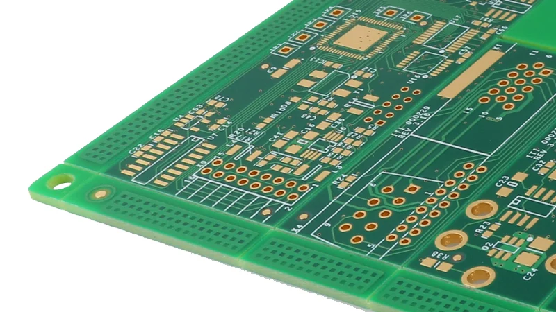
A reliable high-speed PCB manufacturer should therefore be involved before the PCB layout is finalized.
By combining careful material selection, high-speed PCB stack-up design, controlled impedance manufacturing, vacuum lamination, advanced inspection, and reliable testing, manufacturers can reduce the gap between simulated performance and real-world hardware.
With integrated PCB fabrication, PCBA assembly, component sourcing, engineering support, inspection, and production services, Kingda helps customers move high-speed PCB projects from prototype to production while maintaining greater control over quality, manufacturability, and supply-chain consistency.